What Is Electronic Design Automation? Tools, Uses & Future Trends

Summary

  • Market Growth: The global EDA market is projected to expand significantly, driven by the demand for complex ICs in AI, automotive, and 5G sectors.
  • Core Function: Electronic design automation (EDA) replaces manual circuit design with sophisticated software for simulation, verification, and manufacturing preparation.
  • Workflow Essentials: The process moves from logical design and synthesis to physical layout and rigorous verification (DRC/LVS) before fabrication.
  • Manufacturing Impact: EDA tools are critical for fabs and foundries to ensure high yield, reduce “spin” costs, and maintain compatibility with advanced packaging.
  • Future Outlook: AI integration and cloud-based EDA are the next frontier, optimising power, performance, and area (PPA) faster than humanly possible.

Introduction

The complexity of modern microchips is difficult to overstate. A single NVIDIA H100 GPU contains 80 billion transistors. If a human engineer attempted to lay out those transistors manually at a rate of one per second, finishing the design would take over 2,500 years. This impossibility is where electronic design automation steps in. According to Grand View Research (2023), the global EDA market size was valued at USD 11.10 billion in 2022 and is expected to grow at a compound annual growth rate (CAGR) of 9.1% from 2023 to 2030.

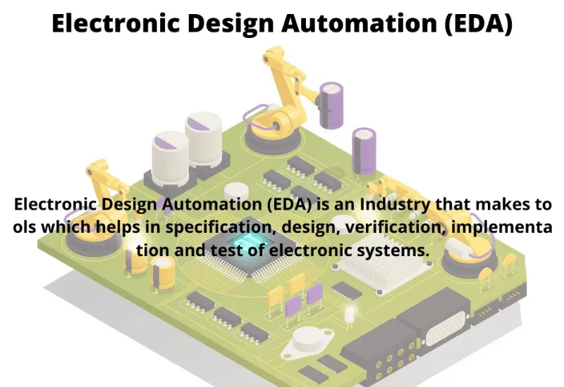
EDA is the backbone of the semiconductor industry. It is a category of software tools used to design electronic systems such as integrated circuits (ICs) and printed circuit boards (PCBs). For semiconductor fabs, foundries, and equipment manufacturers, these tools bridge the gap between a theoretical concept and a physical wafer. Without them, the Industry 4.0 advancements we see in smart factories today would halt immediately.

In this guide, we break down what electronic design automation is, how the workflow functions, and why the future of electronic design automation relies heavily on artificial intelligence and cloud computing.

What Is Electronic Design Automation?

At its core, electronic design automation (EDA) is the software toolchain that enables chip designers to define, plan, design, implement, verify, and manufacture semiconductor devices. Before EDA became standard in the 1980s, integrated circuits were often designed by hand using geometric tapes and manual layout techniques. As Moore’s Law took effect and transistor counts skyrocketed, manual methods became obsolete.

Today, EDA encompasses a massive ecosystem. It covers everything from writing code in Verilog or VHDL to running thermal simulations and finalising the GDSII file sent to the foundry. For a semiconductor automation buyer or a process engineer in a fab, understanding EDA is vital because the output of these tools dictates the manufacturing recipe.

The Nuts and Bolts: How the EDA Workflow Functions

The EDA workflow is a funnel. It starts with abstract logic and ends with a physical blueprint. While every project differs, the standard path involves three main phases.

Design Entry and Simulation

The process begins with the specification. Designers describe the behavior of the chip using a Hardware Description Language (HDL). They do not draw gates yet; they write code.

  • Behavioral Simulation: Engineers test this code to ensure the logic holds up. If the logic says “1 + 1 = 2,” the simulator confirms the output is actually 2.
  • Synthesis: This step translates the abstract code into a gate-level netlist. It converts high-level instructions into actual logic gates (AND, OR, NOT) that can be placed on silicon.

Physical Design (Place and Route)

Once the netlist exists, the chip design software must figure out where to put everything. This is the “Tetris” phase of chip design.

  • Floorplanning: Deciding where major blocks (like the CPU core or memory) go on the die.
  • Placement and Routing: The software places millions of standard cells and connects them with copper wiring (interconnects). The goal is to minimize wire length and optimize signal speed.

Verification and Sign-off

Before a design goes to the fab, it must be perfect. A mistake here costs millions of dollars in wasted wafers.

  • DRC (Design Rule Check): Ensures the layout meets the foundry’s manufacturing constraints (e.g., minimum wire width).
  • LVS (Layout vs. Schematic): Verifies that the physical layout matches the original logical design.
  • Parasitic Extraction: Simulates how electricity will behave in the real physical wires, accounting for resistance and capacitance.

Why Semiconductor Fabs Rely on EDA

For manufacturing units, assembly plants, and OSATs (Outsourced Semiconductor Assembly and Test), EDA is not merely a design tool. It is a yield-protection mechanism.

Reducing Manufacturing Spins

A “spin” refers to running a design through the manufacturing process. If a defect is found after fabrication, the fab must discard the wafers, fix the design, and spin again. Since a single mask set for a 5nm process can cost millions, fabs use rigorous EDA simulations to ensure “first-time-right” silicon.

Compatibility with Advanced Packaging

Modern manufacturing involves complex packaging, such as 2.5D and 3D ICs (stacking chips vertically). Electronic design automation tools now integrate with manufacturing equipment data to predict how heat and stress affect these stacked dies during assembly. This connects directly to smart factory initiatives where equipment connectivity (SECS/GEM) feeds data back to design teams to improve yield.

Note: For factories upgrading to GEM300 standards or retrofitting legacy equipment, the link between EDA data and machine performance is becoming a critical data point for MES integration.

Key Tools in the Chip Design Software Arsenal

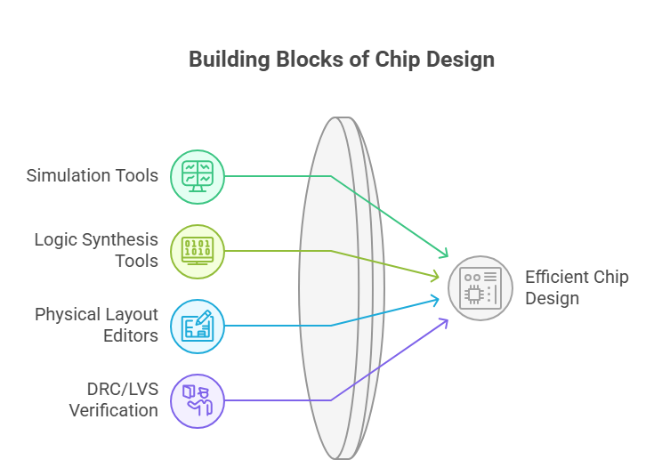
The industry relies on a few heavy hitters for these tasks. While we won’t list every vendor, we can categorize the software types that keep the industry moving.

  1. Simulation Tools: These predict circuit behavior. SPICE (Simulation Program with Integrated Circuit Emphasis) remains the grandfather of all circuit simulators.
  2. Logic Synthesis Tools: These compilers turn code into circuits.
  3. Physical Layout Editors: The CAD tools for drawing the actual polygons on the chip layers.
  4. DRC/LVS Verification Tools: The final gatekeepers before manufacturing.

The Future of Electronic Design Automation

The future of electronic design automation is shifting away from static software toward intelligent, adaptive systems. The demand for lower power consumption and higher performance drives these trends.

AI and Machine Learning in Design

Designers are now using AI to handle the tedious parts of the EDA workflow. Synopsys and Cadence have introduced AI-driven tools that can explore billions of potential layout options to find the optimal arrangement for power and speed.

So, will AI replace the chip designer? Unlikely. AI acts more like a hyper-efficient assistant, handling the “brute force” work of routing wires so engineers can focus on architecture.

Cloud-Based EDA

Historically, companies ran EDA tools on massive on-premise server farms to protect IP. However, the sheer computing power required for 3nm and 2nm designs is pushing the industry toward the cloud. Cloud-based EDA allows small design houses to access supercomputing power on demand, leveling the playing field.

3D-IC and Chiplet Standards

As Moore’s Law slows down, the industry is moving toward “chiplets,” modular dies connected in a single package.EDA tools are evolving to handle the thermal and electromagnetic challenges of putting multiple active chips right next to each other.

Comparison: Legacy vs. Modern EDA

Feature Legacy EDA Modern AI-Driven EDA
Optimization Manual iteration by engineers AI explores the design space automatically
Compute On-premise server farms Hybrid or fully Cloud-native
Focus Single monolithic die Chiplets and 3D-IC packaging
Speed Weeks for physical closure Days or hours for physical closure

Conclusion

Electronic design automation has evolved from a niche drafting aid to the central nervous system of the semiconductor supply chain. For fabs, foundries, and automation engineers, understanding these tools is essential for bridging the gap between digital concepts and tangible silicon. As we move toward 3D-IC structures and AI-integrated manufacturing, the synergy between design software and factory automation will only deepen.

Whether you are retrofitting legacy equipment or building a fully automated smart factory, the data starts with the design.

Contact Us Today

Get Expert Help to Choose the Right EDA Solutions for Your Projects


Introduction to Multivariate SPC: A Beginner’s Guide to MSPC

Summary

  • Traditional Limits: Univariate SPC often fails in complex manufacturing because it treats process variables in isolation, ignoring how they interact.
  • The Multivariate Advantage: MSPC analyzes the relationships between variables, allowing for earlier detection of faults that standard charts miss.
  • Key Metrics: Concepts like Hotelling’s $T^2$ and Squared Prediction Error (SPE) are the backbone of modern fault detection.
  • Techniques: Principal Component Analysis (PCA) and Partial Least Squares (PLS) reduce massive datasets into actionable insights.
  • Real-world Application: From semiconductor fabrication to pharmaceutical batch processing, MSPC prevents false alarms and improves yield.

Introduction

Modern manufacturing creates a staggering amount of data. According to a report by McKinsey (2018), data-driven manufacturing can reduce machine downtime by up to 50% and lower quality costs by up to 20%. Yet, many facilities still rely on charts developed nearly a century ago.

If a factory runs hundreds of sensors, checking them one by one is no longer effective. It is like trying to judge the health of an ecosystem by looking at a single tree. This is where a formal Introduction to Multivariate SPC becomes necessary. As processes become more interconnected, the relationship between variables matters far more than the individual values of those variables.

When engineers ignore these correlations, they face two expensive problems: missing actual defects (Type II errors) or chasing ghosts caused by false alarms (Type I errors).

Moving Beyond the Shewhart Chart

Traditional Statistical Process Control (SPC), often called univariate SPC, works beautifully for simple processes. You have one variable, say, the diameter of a piston, and you track it against an upper and lower limit. If the diameter stays within the lines, the part is good.

However, industrial processes are rarely that simple anymore.

The Problem with Univariate Thinking

In a complex system, variables dance together. In a chemical reactor, as pressure rises, temperature might need to rise specifically to maintain equilibrium.

If you look at the pressure chart alone, it looks normal. If you look at the temperature chart alone, it also looks normal. But if pressure is high and temperature is low, the reaction might fail. Univariate charts will show green lights while the product is being ruined.

Multivariate Statistical Process Control (MSPC) solves this. It does not ask, “Is this variable within limits?” It asks, “Is the relationship between these variables normal?”

Core Concepts of Multivariate SPC

To understand Multivariate SPC, you have to get comfortable with the idea of “variable space.” Instead of plotting data points on a flat line (time series), MSPC plots data in multi-dimensional space.

Hotelling’s $T^2$ Statistic

The most common metric in Multivariate SPC (MSPC) methods is Hotelling’s $T^2$. Think of this as a super-powered version of the standard deviation.

In a univariate chart, you check if a point is more than 3 standard deviations ($3\sigma$) from the mean. In the multivariate world, $T^2$ measures the distance of a data point from the multivariate mean (the center of the data cloud), accounting for the correlation structure.

Mathematically, for a sample vector $x$, the statistic is calculated as:

$$T^2 = (x – \bar{x})’ S^{-1} (x – \bar{x})$$

Where:

  • $x$ is the vector of measurements.
  • $\bar{x}$ is the mean vector.
  • $S^{-1}$ is the inverse of the covariance matrix.

If the $T^2$ value exceeds a calculated limit, the process is out of control, even if every individual sensor reads “normal.”

Squared Prediction Error (SPE)

While $T^2$ tells you if the process has drifted away from the model, the Squared Prediction Error (SPE), sometimes called the $Q$-statistic, tells you if the relationship between variables has broken.

If your process normally dictates that Variable A and Variable B move in sync, and suddenly they move in opposite directions, the SPE value will spike. This is the primary way MSPC detects sensor failures or unusual disturbances.

A Practical Multivariate Statistical Process Control Example

Let’s look at a concrete multivariate statistical process control example involving a semiconductor etching process.

The Scenario:

You are monitoring a plasma etch chamber. Key variables include:

  1. RF Power
  2. Chamber Pressure
  3. Gas Flow Rate

The Univariate View:

  • RF Power: 505 Watts (Upper Limit: 510). Status: OK.
  • Pressure: 42 mTorr (Upper Limit: 45). Status: OK.
  • Gas Flow: 98 sccm (Upper Limit: 100). Status: OK.

A standard control system sees no alarms. The operator assumes the wafer is processing correctly.

The Multivariate View:

Physics dictates that if the Chamber Pressure drops, the Gas Flow Rate usually increases to compensate and maintain plasma density.

In this specific run, Pressure dropped slightly to 42, but Gas Flow also dropped to 98. Individually, these numbers are fine. But together? They are impossible under normal operating conditions. The correlation structure is broken.

An MSPC model would flag this immediately. The $T^2$ chart might remain stable, but the SPE chart would scream a warning. The engineer stops the tool and finds a blockage in the mass flow controller. If they had relied on univariate charts, they would have scrapped a full cassette of wafers.

Contact Us Today

Get Step-by-Step Help to Implement Multivariate SPC

Key Multivariate SPC (MSPC) Methods

Handling data from 50 or 100 sensors requires dimension reduction. You cannot look at a 100-dimensional chart. This is where the heavy lifting algorithms come in.

Principal Component Analysis (PCA)

PCA is the most popular tool for continuous processes. It simplifies data by finding “Principal Components,” new, uncorrelated variables that explain the variance in the data.

  • PC1 (Principal Component 1): Usually explains the biggest chunk of variability (e.g., the overall energy level of the system).
  • PC2 (Principal Component 2): Explains the next biggest chunk (e.g., the balance between reactants).

By monitoring two or three Principal Components instead of 100 raw variables, you get a clean, readable dashboard.

Partial Least Squares (PLS)

While PCA focuses on the input variables ($X$), PLS focuses on the relationship between inputs ($X$) and outputs ($Y$), such as yield or quality.

If you want to know which process parameters are driving your quality defects, PLS is the method of choice. It builds a model that predicts quality based on process data, alerting you when the predicted quality drops below standard.

Why Traditional Industries Are Switching

The adoption of multivariate statistical process control is accelerating. According to IFAC (International Federation of Automatic Control), the complexity of industrial systems has made data-driven monitoring mandatory for competitive yield rates (Qin, 2012).

Reduced False Alarms

Operators eventually ignore alarms if they go off too often without cause. Univariate charts on highly correlated data generate massive amounts of statistical noise. MSPC filters this out. It accounts for the noise, meaning when the alarm rings, it is time to run.

Fault Diagnosis

Knowing that something went wrong is good. Knowing what went wrong is better.

Modern MSPC software includes “contribution plots.” When a $T^2$ or SPE alarm triggers, the software generates a bar chart showing exactly which variable contributed most to the alarm. It points the maintenance team directly to the faulty heater or the drifting sensor.

Note: A system is only as good as the data fed into it. Reliable MSPC starts with proper SECS/GEM equipment integration, along with calibrated sensors and consistent data historian logging.

Implementing MSPC in Your Facility

Starting with Multivariate SPC can feel intimidating, but it follows a logical path.

  1. Data Collection: Gather historical data from a period when the process was running well. This is your “Golden Batch” or reference set.
  2. Model Training: Use software to run PCA or PLS on this historical data. The software defines the correlation structure and calculates the control limits.
  3. Validation: Test the model against a set of data that contains known failures. Does the model catch them?
  4. Online Monitoring: Deploy the model to run in real-time, often supported by dedicated SPC control chart software that compares live data against the reference model.

It is wise to start small. Do not try to model the entire plant at once. Pick one critical unit operation, like a distillation column or a CNC machine, and prove the value there first.

Common Challenges and Misconceptions

Despite the power of Multivariate SPC, it is not a magic wand.

  • The Black Box Fear: Engineers sometimes reject MSPC because they cannot “see” the physical meaning of a Principal Component. Training is essential here. The team needs to trust the math.
  • Linearity Assumptions: Standard PCA assumes linear relationships. If your process is highly non-linear (like pH neutralization), you may need advanced versions like Kernel PCA.
  • Static Models: Processes change. Tool parts wear out; raw material vendors change. An MSPC model needs periodic maintenance to remain accurate.

Conclusion

Manufacturing has moved beyond the capabilities of simple line charts. An Introduction to Multivariate SPC is the first step toward reclaiming control over complex, data-heavy environments. By analyzing the relationships between variables rather than treating them as islands, engineers can spot defects earlier and reduce waste significantly.

Whether you are in semiconductors, pharma, or heavy industry, the transition to MSPC is not a luxury; it is the standard for modern quality assurance.

Contact Us Today

Get Expert Support to Deploy MSPC in Your Manufacturing Process


Understanding Computer Integrated Manufacturing (CIM) and Its Benefits

[vc_row][vc_column][vc_column_text css=””]

Computer Integrated Manufacturing (CIM) is an advanced approach that uses computers to control the entire production process. The concept of CIM was first introduced by Dr. Joseph Harrington in his 1974 book, and since then, it has transformed the way industries design, produce, and deliver products.

Unlike traditional manufacturing, CIM connects all functional areas—designing, analysis, planning, purchasing, cost accounting, inventory management, and distribution—with factory floor functions such as materials handling and process control. This results in a fully integrated system where each department communicates seamlessly, leading to higher efficiency, accuracy, and productivity.

[/vc_column_text][/vc_column][/vc_row][vc_row][vc_column width=”1/2″][vc_column_text css=””]

Benefits of Computer-Integrated Manufacturing (CIM)

Adopting CIM brings measurable benefits to manufacturing organizations. According to the U.S. National Research:

  • Productivity increases by 40–70%
  • Design costs reduce by 15–20%
  • Lead time decreases by 20–60%
  • Work-in-progress (WIP) reduces by 30–60%

The integration of computers minimizes human intervention, reducing errors and delays. Automated processes powered by real-time sensor input enable faster and more reliable manufacturing. This flexibility is particularly useful for industries where precision and speed are critical, such as automotive, aerospace, shipbuilding, and electronics.

[/vc_column_text][/vc_column][vc_column width=”1/2″][vc_single_image image=”37160″ img_size=”full” alignment=”center” css=””][/vc_column][/vc_row][vc_row][vc_column][vc_column_text css=””]

How CIM Works

CIM begins at the product design stage and continues until the final product reaches the customer. It works through closed-loop control systems, where data from sensors and monitors is continuously collected, analyzed, and used to adjust processes.

The system integrates multiple functions, including:

  • Product Design & CAD/CAM Integration – Efficient digital design linked directly to manufacturing equipment.
  • Process Planning – Optimized production sequences based on customer needs.
  • Production Monitoring – Real-time equipment and process tracking.
  • Inventory & Cost Control – Automated tracking of materials and expenses.
  • Sales & Distribution – Smooth information transfer from production to delivery.

This end-to-end integration ensures consistency, quality, and transparency across the entire production chain.


[/vc_column_text][vc_column_text css=””]

Key Components of CIM

Three core components distinguish Computer-Integrated Manufacturing from other methodologies:

  1. Data Management – Systems for storage, retrieval, and manipulation of data for effective decision-making.
  2. Sensing & Control – Mechanisms to monitor processes, detect changes, and adjust accordingly.
  3. Algorithms & Integration – Advanced algorithms that link data processing with control mechanisms to enable automation.

Together, these elements create a flexible, adaptive, and intelligent manufacturing system.

[/vc_column_text][vc_column_text css=””]

Implementing CIM in Modern Industries

For successful CIM implementation, several parameters must be considered:

  • Production Volume – Higher volumes benefit more from CIM automation.
  • Company Expertise – The ability of personnel and management to handle integration.
  • Product Complexity – Whether the product itself requires integrated design and manufacturing.
  • Technology Availability – Use of CAD/CAM, robotics, and ICT systems to support CIM.

Industries such as aviation, automotive, space exploration, and shipbuilding already rely heavily on CIM to meet the demands of high precision and large-scale production.

[/vc_column_text][vc_column_text css=””]

Computer Integrated Manufacturing (CIM) represents the future of smart manufacturing. By connecting every step of the production cycle—from design to sales—CIM ensures faster production, reduced costs, higher quality, and greater flexibility. As industries continue to adopt advanced ICT systems, the role of CIM in driving innovation and competitiveness will only grow stronger.

Companies investing in CIM today are setting the foundation for sustainable, automated, and intelligent manufacturing processes that can adapt to tomorrow’s challenges.

[/vc_column_text][/vc_column][/vc_row]

Fab Automation in Lithography: Driving Higher Yields with FDC and Smart Integration

[vc_row][vc_column width=”1/2″][vc_column_text css=””]

Photolithography is one of the most critical processes in integrated circuit (IC) manufacturing. It records a binary image on a photosensitive material layer applied to a semiconductor wafer. Precision and efficiency in this stage directly influence wafer yield and overall production quality in advanced semiconductor fabs.

To ensure consistent high yields for memory and logic devices, semiconductor fabs increasingly rely on data monitoring, analysis, and automation. Among these, Fault Detection and Classification (FDC) and recipe automation play a pivotal role in optimizing lithography processes.

[/vc_column_text][/vc_column][vc_column width=”1/2″][vc_single_image image=”37154″ img_size=”medium” alignment=”center” css=””][/vc_column][/vc_row][vc_row][vc_column][vc_column_text css=””]

The Importance of Real-Time Monitoring in Lithography

Traditionally, fabs sampled wafers periodically within the production sequence or used test wafers to identify defects. However, this method often delayed problem detection and introduced unnecessary costs.

Today, OEMs integrate sensors and monitors directly into process tools, reducing sampling intervals and improving real-time detection. These inline monitors emulate on-wafer measurements, enabling fabs to interpret tool sensor data quickly and apply corrective measures.

This approach powers fab-wide Fault Detection and Classification (FDC) systems, which:

  • Collect real-time equipment data
  • Compare results with “Golden” benchmark data
  • Trigger automatic responses to prevent defective wafer processing

With automation, fabs no longer need to rely solely on physical inspections, saving significant time and improving troubleshooting accuracy.

[/vc_column_text][/vc_column][/vc_row][vc_row][vc_column][vc_column_text css=””]

How FDC Boosts Yield and Efficiency

By leveraging FDC, fabs can:

  • Detect deviations early and stop wafer processing when poor quality is identified
  • Reduce corrective action time by eliminating guesswork
  • Lower costs by minimizing rework and scrap
  • Improve yield and cycle time with precise corrective measures

Einnosys provides a flexible FDC software system tailored to semiconductor fabs’ needs. This system seamlessly integrates with diverse lithography tools and ensures fabs stay competitive with advanced process control. Learn more here

[/vc_column_text][vc_column_text css=””]

Enhancing Lithography with Metrology and Feedback Loops

Metrology equipment provides vital feedback on overlays and critical dimensions. When integrated with lithography tools, this data helps fabs:

  • Auto-analyze overlay data
  • Feed corrections back into steppers
  • Save significant engineering time
  • Improve wafer yield and throughput

This closed-loop automation ensures consistent quality while minimizing manual intervention.

[/vc_column_text][vc_column_text]

I am text block. Click edit button to change this text. Lorem ipsum dolor sit amet, consectetur adipiscing elit. Ut elit tellus, luctus nec ullamcorper mattis, pulvinar dapibus leo.

[/vc_column_text][vc_column_text css=””]

Experience Across Global Lithography Tools

Einnosys brings decades of expertise across multiple lithography equipment, including:

  • Steppers – Canon, ASML, Nikon
  • Tracks – TEL, SVG, DNS
  • Metrology tools – KLA-Tencor, Rudolph, Inspectrology

This extensive experience allows Einnosys to design and deploy automation solutions that work seamlessly with diverse fab ecosystems.

[/vc_column_text][vc_column_text css=””]

Recipe Management and Stepper Job Automation

Another key challenge in lithography is manual job creation, which can lead to errors and inefficiencies. By automating stepper job creation directly from CAD data, fabs eliminate human error and accelerate job setup.

Einnosys’ Recipe Management System (EIRMS) integrates with CAD systems to generate stepper jobs automatically and transfers them to lithography equipment—similar to a JobServer approach. This automation improves accuracy, reduces cycle time, and ensures consistency across production lines. – more here

Lithography remains the backbone of semiconductor manufacturing, and fabs that adopt automation, FDC, and recipe management solutions can achieve significant gains in efficiency, yield, and cost-effectiveness. With its proven expertise and innovative solutions, Einnosys helps fabs worldwide stay ahead in the race for smarter, more productive semiconductor manufacturing.


[/vc_column_text][/vc_column][/vc_row]

Understanding SECS/GEM Data Polling and Its Role in Semiconductor Manufacturing

[vc_row][vc_column][vc_column_text css=””]

In modern semiconductor fabs, efficiency, traceability, and automation depend heavily on seamless communication between equipment and factory host systems. This is where SECS/GEM standards play a critical role. SECS (SEMI Equipment Communications Standard) and GEM (Generic Equipment Model) together define how semiconductor equipment and host software exchange information for monitoring and control.

One of the essential aspects of this communication is Data Polling—a process that allows the factory host to retrieve real-time equipment data for analysis, decision-making, and process optimization.

[/vc_column_text][/vc_column][/vc_row][vc_row][vc_column][vc_column_text css=””]

What is Data Polling in SECS/GEM?

Data polling refers to the host system requesting information directly from equipment. While hosts often receive data through event reports or trace reports, they sometimes need to poll the equipment for specific values. This ensures that fabs have access to the most up-to-date information, especially for monitoring critical process parameters or troubleshooting.

[/vc_column_text][vc_single_image image=”37149″ img_size=”full” alignment=”center” css=””][/vc_column][/vc_row][vc_row][vc_column][vc_column_text css=””]

Categories of Data Items in SECS/GEM

The SECS/GEM standard defines three main categories of data items, each serving a unique purpose in communication.

1. Status Variables (SV)

Status variables represent the real-time condition of equipment or its components.

  • Examples: Temperature, Pressure, Gas Flows, RF Forward Power, Spin Speed.
  • These variables are not tied to events such as lot or wafer starts.
  • The host can request them anytime or set up a trace data report for continuous monitoring.
  • SVs cannot be modified by the host; they only provide a snapshot of equipment conditions.

2. Data Value Variables (DV)

Data value variables are tied to specific events during manufacturing.

  • Examples: LotID, SlotNumber, CurrentRecipe, AlarmID.
  • These variables change only when an event occurs, such as starting a lot or selecting a recipe.
  • The host queries DVs by defining reports and associating them with events.

Unlike SVs, these variables may sometimes have no value—for instance, AlarmID may be empty if no alarms have occurred since the equipment was powered on.

3. Equipment Constants (EC)

Equipment constants define the configuration parameters of the equipment.

  • Examples: PumpDown Time Limit, Equipment Standby Time, Pins Up Wait.
  • Unlike SVs and DVs, a host can modify ECs using SECS messages.

ECs ensure that equipment settings align with factory requirements, supporting customization and optimization.

Properties of SECS/GEM Data Items

Each SECS/GEM data item is defined with certain properties to ensure clarity and consistency:

  • ID – A unique identifier (SVID for status variables, DVID for data variables, ECID for equipment constants).
  • Name – A readable label to make identification easier.
  • Format – Defines the data type: numeric, ASCII, Boolean, arrays, lists, or structures.
  • Value – The actual real-time or event-based data in binary format for efficiency.

This structured approach ensures interoperability and smooth communication across different fabs and equipment suppliers.

How Data Polling Works in Practice

The host may poll equipment data on demand, for example, to check current chamber temperature or pressure before starting a batch.

It can also schedule periodic polling using trace reports, which automatically send updates at defined intervals.

Polling is especially useful for troubleshooting, predictive maintenance, and optimizing process recipes.

By combining event-driven data with polled data, fabs gain a more complete picture of equipment performance, enabling smarter decisions and higher productivity.

[/vc_column_text][/vc_column][/vc_row][vc_row][vc_column][vc_column_text css=””]

Why Data Polling Matters

  • Operational Efficiency – Ensures critical parameters are always monitored.
  • Traceability – Maintains accurate logs for audits and compliance.
  • Flexibility – Allows hosts to fetch exactly the data needed, when needed.
  • Reliability – Supports predictive maintenance by providing early warnings of deviations.

[/vc_column_text][/vc_column][/vc_row][vc_row][vc_column][vc_column_text css=””]

Conclusion

The SECS/GEM standard has transformed semiconductor manufacturing by establishing a universal communication protocol. Within it, Data Polling serves as a vital tool that empowers fabs to collect accurate, real-time data from equipment, complementing event reports and trace data.

By leveraging polling along with other SECS/GEM features, fabs can achieve improved monitoring, faster response times, and higher levels of automation—driving the semiconductor industry toward greater efficiency and innovation.

[/vc_column_text][/vc_column][/vc_row]

Fab Automation Standards: SECS/GEM Compliance & Retrofit Solutions


Summary

  • Market Context: The semiconductor market is projected to hit nearly $1 trillion by 2030, making automation critical for meeting demand (McKinsey, 2023).
  • The Challenge: Mixed fleets of modern and legacy equipment create communication silos, hindering data collection and process control.
  • The Solution: Adopting fab automation standards like SECS/GEM and GEM300 ensures seamless equipment-to-host communication.
  • Legacy Retrofits: Einnosys provides hardware and software solutions to make non-compliant “dumb” tools smart without expensive replacements.
  • Key Benefits: Enhanced yield management, reduced scrap, and a clear path to Industry 4.0 compliance.

Introduction

The semiconductor industry is sprinting. According to McKinsey (2023), the global semiconductor market is poised to reach $1 trillion by 2030. To keep up with this insatiable demand, manufacturers cannot rely on manual data entry or siloed machinery. Efficiency is the only currency that matters.

Yet, a surprising number of production floors still struggle with equipment that refuses to “talk” to the central management system. This disconnect often stems from a lack of adherence to fab automation standards. When machines cannot communicate their status, alarms, or process data to the Manufacturing Execution System (MES), production slows down. Errors creep in. Yields drop.

For any facility, whether it is a cutting-edge 300mm wafer fab or a specialised LED manufacturing plant, establishing a universal language for equipment is non-negotiable. That language is defined by the SEMI standards, specifically SECS/GEM. This article breaks down these protocols and explores how Einnosys solutions bridge the gap between mute machinery and a fully connected smart factory.

Decoding the Alphabet Soup: What is SECS/GEM?

If you have ever tried to get a Windows PC to talk to a printer from the early 2000s without the right driver, you understand the pain of equipment integration. In a fab, the stakes are significantly higher than a stuck paper tray.

Fab automation standards are the agreed-upon protocols that allow different machines from different vendors to communicate with a host computer. The most prevalent of these is SECS/GEM.

The Two Parts of the Equation

  • SECS (Semiconductor Equipment Communication Standard): This handles the transport of data. It defines how messages get sent over a connection (usually RS-232 or TCP/IP). It breaks down into SECS-I (serial) and HSMS (High-Speed SECS Message Services for Ethernet).
  • GEM (Generic Model for Communications and Control of Manufacturing Equipment): This handles the behaviour. It defines what the machines should say. GEM ensures that when the host asks for a “Status Variable,” every machine responds predictably.

Without GEM, an etcher might report temperature in Celsius while a deposition tool reports it in Kelvin, and neither would tell you when they finished a batch. Fab automation standards SECS/GEM harmonise this chaos.

Why This Protocol Rules the Floor

Why do we still use a standard developed decades ago? Reliability.

SECS/GEM is robust. It allows for:

  1. Remote Control: Starting and stopping processing jobs from a control room.
  2. Alarm Management: Instant notification if a process variable goes out of spec.
  3. Data Collection: Gathering critical metrology data for yield analysis.
  4. Recipe Management: Uploading the correct process recipe directly to the tool to prevent human error.

Does your toaster need this level of control? Probably not. But for semiconductor fab automation, where a single misstep ruins distinct wafers worth thousands of dollars, it is mandatory.

Scaling Up: GEM300 and Interface A

As the industry moved from 200mm to 300mm wafers, the logistics became too complex for basic GEM. Moving a cassette of 25 wafers (a FOUP) became a job for automated material handling systems (AMHS), not humans.

The GEM300 Standard Suite

To handle full fab automation, the GEM300 standards were introduced. These include:

  • E39 (Object Services): dealing with data as objects.
  • E40 (Process Job Management): tracking the processing of specific wafers.
  • E87 (Carrier Management): managing the movement of the FOUPs (Front Opening Unified Pods) to and from the load ports.
  • E90 (Substrate Tracking): keeping tabs on individual wafers within the carrier.

For a modern 300mm fab, compliance with these standards is the difference between a synchronised ballet of robots and a collision-prone disaster.

Interface A (EDA)

While SECS/GEM is great for control, it can get clogged if you try to pull massive amounts of data for high-frequency analysis. Enter Interface A (Equipment Data Acquisition).

Interface A runs alongside SECS/GEM but is dedicated solely to data collection. It enables fab automation manufacturing teams to pull high-speed data for fault detection without slowing down the tool’s control operations.

The Legacy Equipment Challenge

Here is the reality for many factories: you are not building a greenfield fab from scratch. You likely have a mix of brand-new tools and reliable workhorses that have been running since the late 90s.

According to a report by the SEMI Foundation (2022), a significant portion of the global capacity for 200mm wafers relies on legacy equipment. These machines cut silicon perfectly well, but their computers are ancient. Some run on Windows 98. Some have no Ethernet ports. Some lack the software capable of speaking SECS/GEM.

The “Dumb” Machine Problem

When a machine cannot connect to the MES, it creates a “black hole” in your data.

  • Operators must manually type in lot numbers (prone to typos).
  • Engineers cannot see real-time performance.
  • Recipe selection is manual, leading to the dreaded “wrong recipe” scrap event.

For fab automation assembly lines in LED or PV manufacturing, replacing these expensive tools just to get connectivity is financial suicide. The ROI generally does not exist.

So, how do you modernise without buying new?

Einnosys Solutions: Bridging the Gap

This is where Einnosys steps in. We specialise in making the impossible connections possible. We understand that adhering to fab automation standards shouldn’t require scrapping functional equipment.

EIGEM – The SECS/GEM Driver

For equipment manufacturers (OEMs) building new tools, writing the SECS/GEM code from scratch is a massive headache. It distracts developers from focusing on the core process technology.

EIGEM is our library/driver solution. It is a plug-and-play software component that OEMs can integrate into their equipment control software. It instantly makes the machine compliant with fab automation standards SECS/GEM and GEM300. It supports C#, C++, Java, and Python, making integration smooth regardless of the base architecture.

Retrofitting with Hardware Adapters

For the factories holding onto those legacy tools, software alone often isn’t enough. If the machine’s controller is a proprietary black box or an ancient PLC, you need an intermediary.

Einnosys provides smart hardware adapters (E-Box) that act as a translator.

  1. Connection: We connect to the tool’s internal signals (via analogue/digital I/O, PLC registers, or log files).
  2. Translation: The E-Box interprets these signals: “The heater is on,” “The door is open.”
  3. Communication: The adapter converts these states into standard SECS/GEM messages and sends them to the factory host.

To the MES, the 30-year-old sputtering machine now looks and acts like a brand-new, smart-compatible tool.

Contact Us Today

Get Step-by-Step Help for SECS/GEM Compliance & Retrofit


Key Benefits of Standardisation

Why go through the trouble? Why invest in retrofitting or upgrading to these standards?

Yield and Quality Control

When you automate recipe selection via SECS/GEM, you eliminate the “fat finger” error. An operator cannot accidentally select the “High Temp” recipe for a “Low Temp” lot if the host computer prevents it.

Furthermore, with automated data collection, process engineers can spot drifts in temperature or pressure before they ruin the batch.

Operational Efficiency (OEE)

You cannot improve what you do not measure. By bringing all equipment under fab automation standards, you gain visibility into:

  • Idle Time: Is the machine waiting for a distinct operator?
  • Down Time: How often does the vacuum pump fail?
  • Throughput: Are we meeting the targets per hour?

This data feeds directly into OEE (Overall Equipment Effectiveness) calculations, allowing management to pinpoint bottlenecks.

Future-Proofing for Industry 4.0

The buzzword “Industry 4.0” is thrown around often, but it essentially means using data to make smart decisions. AI and Machine Learning models need clean, structured data.

If your data comes from manual Excel sheets, your AI models will fail. Fab automation standards ensure that the data feeding your advanced analytics is accurate, timely, and standardised.

Implementation: How to Get Started

Transforming a fab into a smart factory is not an overnight event. It requires a strategic approach.

Assessment and Audit

Start by auditing your floor.

  • Which machines are already GEM compliant?
  • Which machines have GEM but need it enabled?
  • Which machines are “dumb” and need a retrofit box?

Partnering for Success

Don’t try to build a SECS/GEM driver in-house unless you have a team of developers with nothing else to do. It is a complex protocol with hundreds of edge cases.

Partnering with experts like Einnosys allows your internal teams to focus on process engineering while we handle the connectivity. Whether you are an OEM needing a library for a new wire bonder or a fab manager trying to connect a fleet of legacy ovens, we have the specific toolset required.

Conclusion

The semiconductor landscape is unforgiving. As feature sizes shrink and production volumes swell, the margin for error vanishes. Adhering to fab automation standards is no longer a luxury for the elite 300mm fabs; it is a survival requirement for every manufacturing unit in the supply chain.

From enabling basic communication with SECS/GEM to managing complex logistics with GEM300, these protocols form the nervous system of the modern factory. And for the equipment that time forgot, Einnosys offers the bridge to bringing them into the future.

Contact Us Today

Get Expert Guidance to Upgrade Your Equipment to SECS/GEM Standards

SECS/GEM Simulator Introduction and Features

[vc_row][vc_column width=”1/2″][vc_column_text css=””]In semiconductor manufacturing, reliable communication between equipment and host systems is essential for productivity, compliance, and automation. SECS/GEM (SEMI Equipment Communication Standard / Generic Equipment Model) provides the foundation for this communication. However, validating SECS/GEM implementation on new or legacy equipment can be time-consuming and complex.

To address this, EINNOSYS has developed EIGEMSim, a powerful SECS/GEM simulator designed to help OEMs, fabs, and assembly/test facilities test and verify SEMI compliance. With EIGEMSim, engineers can simulate both equipment and factory host environments, making it an indispensable tool for development, integration, and testing.[/vc_column_text][/vc_column][vc_column width=”1/2″][vc_single_image image=”37139″ img_size=”full” alignment=”center” css=””][/vc_column][/vc_row][vc_row][vc_column][vc_column_text css=””]What is EIGEMSim?

EIGEMSim is a software application that allows seamless testing of SECS/GEM communication. Depending on the use case, it can be configured to act either as the equipment or as the factory host. This flexibility enables teams to validate their integration scenarios without requiring a physical host system or equipment during early development stages.

The simulator supports creation, configuration, transmission, and receipt of SECS messages. To simplify operations, EIGEMSim uses a Message Dictionary, which facilitates message transfers and ensures accuracy in communication testing.[/vc_column_text][vc_column_text css=””]Creating and Configuring SECS Messages

One of the strengths of EIGEMSim is its flexibility in creating and configuring messages. Engineers can:

Use a built-in wizard that guides them step-by-step in defining SECS messages.

Or, write messages in SML (SEMI Markup Language) format using any text editor and then import the SML file directly into EIGEMSim.

This dual approach caters to both beginners and advanced users, providing efficiency and control during development. All messages sent and received are automatically logged, giving developers a complete record for analysis and troubleshooting.[/vc_column_text][/vc_column][/vc_row][vc_row][vc_column][vc_column_text css=””]Key Features of EIGEMSim

EIGEMSim comes packed with features that simplify SECS/GEM compliance testing and integration:

✅ Cross-Platform Support – Runs seamlessly on both Windows and Linux environments.

✅ Pre-Configured Messages – Includes the most commonly used SECS messages, helping users start compliance testing quickly.

✅ User-Friendly Interface – Intuitive design for easy configuration and message transmission.

✅ Dual Configuration – Can be set up as equipment or factory host, depending on the testing scenario.

✅ Comprehensive Logging – Records all incoming and outgoing messages for review, debugging, and documentation.[/vc_column_text][/vc_column][/vc_row][vc_row][vc_column][vc_column_text css=””]Why Choose EIGEMSim?

For OEMs and fabs, validating SEMI compliance is critical before deploying equipment in production environments. Traditional testing methods can be slow and require multiple hardware components. EIGEMSim removes these bottlenecks by providing a software-only, configurable simulator that reduces both time-to-market and testing costs.

With its ability to simulate different roles (equipment or host) and its ready-to-use message library, EIGEMSim accelerates development while ensuring compliance with SEMI SECS/GEM standards.

SECS/GEM integration is at the heart of modern semiconductor factory automation, and reliable testing tools are key to ensuring success. EIGEMSim by EINNOSYS empowers equipment manufacturers, fabs, and assembly/test facilities to streamline compliance testing, reduce complexity, and achieve faster integration.

Whether you’re developing new semiconductor equipment, upgrading legacy systems, or validating host communication, EIGEMSim offers the flexibility and reliability you need.

👉 Learn more about EIGEMSim and other SECS/GEM solutions from EINNOSYS at einnosys.com[/vc_column_text][/vc_column][/vc_row]

Understanding SEMI, SECS, and GEM Standards in Semiconductor Manufacturing

In the world of semiconductor manufacturing, communication between equipment and factory systems is critical for efficiency, automation, and cost control. To make this communication seamless, the industry relies on well-defined standards known as SEMI, SECS, and GEM. Let’s take a closer look at what these terms mean and why they matter.

What Do SEMI, SECS, and GEM Stand For?

SEMI – Semiconductor Equipment and Materials International, an organization that develops global standards for semiconductor and electronics industries.

SECS – Semiconductor Equipment Communication Standard, which defines how semiconductor equipment communicates with host systems.

GEM – Generic Equipment Model, a set of guidelines for communications and control of manufacturing equipment.

Together, SECS/GEM standards ensure a common “language” for equipment-to-host communication in fabs and assembly facilities.[/vc_column_text][/vc_column][vc_column width=”1/2″][vc_column_text css=””]Why Were SECS/GEM Standards Introduced?

The semiconductor industry began adopting automation standards in the 1970s. At that time, communication between equipment and factory hosts was often proprietary, inconsistent, and expensive to implement.

Without a standard, every equipment manufacturer had to design unique communication protocols for each fab, leading to:

High development and integration costs

Performance issues

Longer equipment setup times

SEMI addressed this by introducing SECS/GEM standards—a unified way for equipment and hosts to exchange information. Much like how TCP/IP standardizes network communication or RS232 standardizes serial communication, SECS/GEM created a universal framework for semiconductor automation.

How Do SECS/GEM Standards Work?

The SECS/GEM standard must be implemented on both sides of the communication:

On the Equipment Side – The equipment’s computer runs SECS/GEM software that complies with SEMI standards such as E30, E4, E5, and E37. This software manages message formats, event reporting, and remote commands.

On the Host Side – The factory host software also implements the same SEMI standards. This ensures that the host can send commands, receive data, and control the equipment reliably.

By ensuring both sides “speak the same language,” fabs and equipment manufacturers achieve seamless interoperability.[/vc_column_text][/vc_column][/vc_row][vc_row][vc_column][vc_column_text css=””]Benefits of SECS/GEM Standards

Implementing SECS/GEM provides significant advantages to both fabs and OEMs:

Interoperability – Equipment from different vendors can easily integrate with fab automation systems.

Reduced Costs – No need for custom protocols or one-off integrations.

Faster Deployment – Standardized communication shortens installation and validation time.

Improved Efficiency – Consistent data collection, event reporting, and control functions enhance overall manufacturing productivity.

Scalability – As fabs adopt more automation, SECS/GEM ensures that new equipment fits into the existing ecosystem.[/vc_column_text][/vc_column][/vc_row][vc_row][vc_column][vc_column_text css=””]Why SECS/GEM Matters Today

Even decades after its introduction, SECS/GEM remains the foundation of smart manufacturing in semiconductors. Modern fabs are highly automated, with thousands of tools connected to centralized host systems. Without a standard protocol, this level of integration would be impossible.

As factories adopt AI, predictive maintenance, and advanced analytics, reliable and standardized data from equipment becomes even more important. SECS/GEM ensures that this data flows consistently, enabling fabs to optimize yield, reduce downtime, and stay competitive.

Conclusion

The SEMI SECS/GEM standards transformed semiconductor manufacturing by creating a universal framework for equipment and host communication. By eliminating proprietary protocols, these standards reduced costs, improved efficiency, and paved the way for today’s advanced automation.

For fabs and OEMs, adopting SECS/GEM isn’t just about compliance—it’s about ensuring smooth integration, scalability, and long-term success in a rapidly evolving industry.

To learn more about SECS/GEM integration solutions, explore Einnosys SECS/GEM products and services[/vc_column_text][/vc_column][/vc_row]