SECS/GEM을 GEM이 아닌 장비에 통합: 실용적인 엔지니어 가이드

요약

  • 과제: 레거시 또는 비표준 장비를 현대 반도체 및 첨단 제조 공장의 자동화 시스템에 연결하는 것은 가장 어려운 과제 중 하나입니다. 
  • 표준: SECS/GEM(SEMI Equipment Communications Standard/Generic Equipment Model)은 현대 팹에서 호스트-장비 통신을 위해 필수적으로 요구되는 표준 프로토콜입니다. 
  • 목표: 이 가이드는 공장 자동화 엔지니어 및 OEM 장비 제작자가 원래 SECS/GEM 기능이 없는 장비에 SECS/GEM 통합을 구현할 수 있도록 실질적인 절차를 제공합니다.
  • 해결책: 해결책은 보통 “GEM Wrapper” 또는 “Gateway”라고 불리는 소프트웨어 계층을 생성하여 장비의 고유 제어 신호를 표준화된 SECS/GEM 메시지로 변환하는 것입니다.
  •  주요 단계: 제어 포인트 식별, 이벤트 및 알람 매핑, 새로운 Host Communication Interface(HCI)가 안정성과 SECS/GEM 규격을 준수하는지 철저히 테스트하는 단계가 포함됩니다.

소개

반도체 및 첨단 제조 산업은 정밀성과 표준화된 통신 위에서 운영됩니다. 이 통합의 핵심에는 SECS/GEM(SEMI Equipment Communications Standard/Generic Equipment Model)이 있으며, 이는 중앙 호스트 컴퓨터(MES 등)가 생산 장비를 관리하고 모니터링할 수 있게 해주는 사실상의 국제 표준 프로토콜입니다.

그러나 모든 장비가 이 언어를 유창하게 구사하는 것은 아닙니다. 현대 표준 이전에 제작된 레거시 장비, 독자적 인터페이스를 가진 커스텀 장비, 소규모 OEM 장비 등은 기본적으로 SECS/GEM을 지원하지 않습니다. 이러한 “non-GEM” 장비를 자동화된 최신 팹 환경에 통합하는 것은 공장 자동화 엔지니어가 반드시 해결해야 하는 과제입니다.

McKinsey & Company(2023)의 반도체 제조 보고서에 따르면 레거시 장비를 자동화하면 처리량과 가동시간 측면에서 20% 이상의 효율 향상이 가능하다고 합니다. 이는 통합의 경제적 가치가 매우 크다는 뜻입니다.

문제는 다음과 같습니다:
어떻게 이 통신 격차를 실제로 메울 것인가?

이 가이드는 내부 API, 시리얼 포트, TCP/IP 소켓, PLC I/O 등 어떤 고유 인터페이스를 사용하는 장비라도 SECS/GEM 통합을 구현할 수 있도록 단계별 실무 절차를 제공합니다. 목표는 기존에 연결되지 않았던 장비를 완전한 자동화 환경에 통합된, SECS/GEM 준수 장비로 변화시키는 것입니다.

Non-GEM 문제: 통합이 필수적인 이유

반도체처럼 고속·고자본 산업에서 장비가 자신의 상태를 통신하지 못한다는 것은 곧 비용이 발생한다는 의미입니다.

Non-GEM 장비는 보통 다음과 같은 문제를 일으킵니다:

  • 수동 데이터 수집
  • 오류 보고 지연
  • MES가 중요한 공정 명령을 전송할 수 없음

따라서 표준화된 Host Communication Interface(HCI)는 필수입니다.

연결 끊김 인식: 일반적인 Non-GEM 인터페이스

솔루션으로 들어가기 전에 장비가 현재 “어떤 언어를 사용하는지” 이해하는 것이 중요합니다. 통합 계층(Wrapper)은 이 언어를 “듣고” SECS/GEM으로 번역해야 합니다.

독점 API/SDK:

 대형 OEM 장비는 TCP/IP 기반의 고유 라이브러리(API 또는 SDK)를 제공하기도 합니다. 구조화되어 있으나 복잡도가 높습니다.

산업용 프로토콜:

 Modbus, EtherNet/IP, Profibus 등 PLC 기반 제어용 산업용 프로토콜을 사용할 수 있습니다.

간단한 I/O 및 직렬 포트:

 레거시 장비는 디지털/아날로그 I/O, RS-232 시리얼 통신 기반인 경우가 많습니다.
예: “Running,” “Error,” “Ready”

데이터베이스 폴링:

특정 커스텀 장비는 상태/제어 정보를 SQL 기반 DB(MSSQL, MySQL)에 기록하는 방식일 수 있습니다.

핵심 문제는 다음과 같습니다:
이들 인터페이스는 SEMI 표준 메시지 구조(SECS-II 등)를 따르지 않습니다.

연결 구축: SECS/GEM 래퍼 아키텍처

비표준 장비를 GEM 호환 장비로 만드는 가장 현실적이고 일반적인 접근법은 “GEM Wrapper” 또는 “SECS Gateway” 소프트웨어를 구축하는 것입니다.

GEM 래퍼의 핵심 기능

Wrapper는 번역기 역할을 하며 다음 두 가지 방향의 기능을 수행합니다.

호스트-장비(MES 다운스트림):

  • SECS/GEM 메시지 수신 (예: S2F41: Host Command Send)
  • 이를 장비가 이해하는 내부 명령 형식으로 변환
  • 예: 고유 API에 문자열 명령 전송

장비-호스트(MES 업스트림):

  • 장비의 고유 인터페이스 감시
    (예: Modbus 레지스터 polling, 시리얼 포트 listening)
  • 상태 변화 발생 시 이를 SECS/GEM 메시지로 변환
    (예: S6F11: Event Report)

이 계층은 고유 인터페이스의 복잡성을 숨기고 호스트에는 “완전한 SECS/GEM 장비”처럼 보이도록 합니다.

SECS/GEM 통합을 위한 실제 엔지니어링 워크플로우

통합 작업은 구조화된 엔지니어링 프로세스를 따라야 하며 특히 데이터 매핑과 에러 처리 설계가 중요합니다.

1단계: 기본 인터페이스 심층 분석 및 데이터 매핑

첫 단계이자 가장 시간이 많이 드는 작업은 고유 인터페이스 구조를 완전히 분석하고 상세 데이터 맵을 만드는 것입니다.

A. 통제점 식별

호스트가 장비에 보낼 수 있는 명령 정의
예: Start, Stop, Pause, Abort, Recipe Download

B. 장비 변수 매핑(데이터 항목)

호스트가 모니터링해야 하는 주요 값
예:

  • Current Recipe Name
  • Chamber Temperature ($T_{Chamber}$)
  • Wafer Count
  • $O_2$ Flow Rate
  • Status (Idle, Setup, Run, Down)

각 항목에 SECS ID(EVID, CEID, SVID) 부여

C. 이벤트 및 알람 정의

장비 상태 변화(Event), 비정상 상황(Alarm)을 매핑
예:

  • Event: Process Start → Native code 100 → GEM CEID 501
  • Alarm: Over-Temperature → Native error T-99 → GEM ALID 1021

일화:

 레거시 문서는 종종 30년 전 돌에 새겨놓은 듯합니다.
“Wafer Out 신호가 깜빡이는 LED라고?” 같은 순간이 매우 흔합니다.

이 매핑 문서가 해당 비표준 장비의 Generic Equipment Model이 됩니다.

2단계: GEM 래퍼 개발 및 구현

매핑이 완료되면 소프트웨어 개발 단계로 이동합니다.
C#, Java, Python 등 고급 언어 + 상업용 SECS/GEM SDK 사용을 강력히 추천합니다.

메시지 번역 논리

예: S2F49: Equipment Constant Write 처리 절차

  • ECID 확인 (예: ECID 100 = $T_{set}$)
  • SECS 메시지에서 값 추출
  • 장비 인터페이스 명령 형식으로 변환
    (예: Modbus register 40001 write)
  • 장비에 명령 전송
  • 성공/실패 ACK를 S2F50으로 반환

상태 머신 구현

Wrapper는 SECS/GEM Equipment Status Model을 구현해야 합니다.
이는 SEMI E30에서 정의한 유한 상태 기계(FSM)입니다.

예:
$EQP_IDLE → EQP_RUN → EQP_SETUP$

Wrapper는 고유 인터페이스를 모니터링하여 장비 활동을 기반으로 상태를 전환해야 합니다.

3단계: 엄격한 규정 준수 및 신뢰성 테스트

레트로핏 통합에서는 테스트가 개발보다 더 중요합니다.

규정 준수 테스트

  • SECS/GEM 시뮬레이터를 사용해 모든 메시지/쿼리 테스트
  • 이벤트/알람/변수가 정확하고 적시에 보고되는지 확인
  • OEM 수준의 SECS/GEM 호환성 확보

스트레스 테스트

  • MES가 고주파수로 요청을 보내도 안정적으로 동작해야 함
  • 데이터 유실, 크래시 없어야 함

고장 및 복구 테스트

예:

  • 네트워크 끊김
  • 공정 중 장비 전원 다운
  • 통신 타임아웃

Wrapper는 SEMI E30의 link test 및 복구 절차를 구현해야 합니다.

Funny Anecdote:
어떤 팹은 일주일간 버그를 찾다 결국 원인이 “시리얼 케이블 뽑아서 휴대폰 충전한 기술자”였다는 사실을 발견했습니다.
항상 물리 레이어부터 확인하세요!

맞춤화의 역할과 공장 자동화 통합의 미래

Non-GEM 통합 프로젝트는 장비별로 모두 다릅니다.
자동화 프로토콜, MES 요구사항에 따라 상당한 커스터마이징이 필요합니다.

기본 통합 그 이상: 고급 GEM 기능

기본 통신이 구축되면 고급 기능을 구현해 장비의 가치를 최대화할 수 있습니다.

레시피 관리 (S7F1–S7F26)

  • MES가 레시피 업로드/다운로드/관리
  • 수동 입력 제거 → 인간 오류 감소

데이터 튜닝 및 추적 (S6F1, S2F23)

  • SPC용 고주파수 데이터 수집
    예: 100ms마다 chamber pressure

공정 프로그램 선택

  • 제품마다 정확한 레시피 버전 자동 선택

이 기능들은 단순 모니터링을 넘어서
실제 폐루프 제어(Closed-loop Control)
를 가능하게 합니다.

Contact Us Today

비-GEM 장비 개조 및 자동화를 위한 전문가 가이드 받기

결론

GEM Wrapper를 사용한 Non-GEM 장비 통합은 쉽지 않지만 공장의 운영 능력을 근본적으로 향상시키는 필수 작업입니다.
데이터 매핑 → Wrapper 개발 → 규격 준수 테스트까지 방법론적으로 수행하면 레거시/비표준 장비도 최신 자동화 환경에 완벽히 통합할 수 있습니다.

이는 설비의 수명을 연장하고 효율성을 크게 향상시키며 SECS/GEM 통합 비용을 여러 번 상쇄하는 투자입니다.


SECS/GEM Plan-B 서비스: 안정적인 Fab 자동화를 위한 백업 통신 솔루션

요약

  • SECS/GEM Plan-B는 반도체 제조 장비를 위한 페일오버(failover) 통신 프로토콜로 작동합니다.
  • 이 서비스는 기본 HSMS 링크가 장애가 발생할 때에도 장비와 호스트(MES) 간 데이터 흐름이 지속되도록 보장합니다.
  • SECS/GEM 이중화(백업)를 구현하면 웨이퍼 스크랩 및 예기치 않은 다운타임 위험을 줄일 수 있습니다.
  • SEMI E30 표준에 따라 Plan-B는 진단 및 백업을 위한 보조 연결 포트를 허용합니다.
  • 이 솔루션은 통신 장애 시 분당 수천 달러의 손실이 발생하는 고산출량 300mm 팹에서 특히 중요합니다.

소개

SEMI(2024)에 따르면 글로벌 반도체 장비 시장은 1,063억 달러라는 사상 최고치를 기록했으며, 이는 업계 전반에서 최대 처리량과 안정성을 향한 강한 수요를 반영합니다. 팹 규모가 커질수록 계획되지 않은 다운타임의 비용은 치솟으며, 일부 고산출 라인의 경우 시간당 38,000달러를 초과하기도 합니다. 이러한 고위험 환경에서 SECS/GEM 프로토콜은 디지털 신경망 역할을 하지만, 가장 견고한 기본 연결조차도 장애가 발생할 수 있습니다.

 작은 네트워크 글리치나 호스트 시스템 오류는 공장을 사실상 ‘눈먼 상태’로 만들며, 생산 중단 또는 심각한 웨이퍼 스크랩을 초래할 수 있습니다. 이러한 위험을 완화하기 위해 업계는 점점 더 “Plan B” 방식을 채택하고 있습니다. 이 보조 통신 전략은 기본 링크가 끊겼을 때도 데이터가 흐르는 안전망 역할을 합니다.

 본 문서는 SECS/GEM 백업 서비스의 기술적 구조와 현대 반도체 제조에서 필수 요소가 된 이유를 설명합니다. 장비 엔지니어이든 팹 자동화 전문가이든, 위기 상황에서도 장비 연결을 유지하는 방법을 이해하는 것은 운영 우수성을 위해 매우 중요합니다.

기본 HSMS 연결의 취약성 이해

High-Speed SECS Message Services(HSMS)는 TCP/IP 기반 SECS 메시지 전송을 위한 업계 표준입니다. HSMS는 빠르고 효율적이지만 포인트 투 포인트 방식으로 동작하기 때문에 구조적으로 취약합니다. 호스트 컴퓨터가 재부팅되거나 네트워크 스위치가 고장 나면 장비는 MES와의 연결을 즉시 잃게 됩니다.

단일 링크가 실패하는 이유

일반적인 팹 환경에서 하나의 장비-호스트 링크가 공정 레시피, 알람 모니터링 등 모든 기능을 처리합니다. 이 링크가 끊기면 장비는 데이터를 로컬로 저장하는 “spooling” 모드로 들어가지만 스풀링에는 한계가 있습니다. 버퍼가 가득 차기 전에 연결이 복구되지 않으면 중요한 공정 데이터가 영구적으로 손실됩니다.

의사소통 실명으로 인한 비용

연결 상실은 단순한 불편을 넘어섭니다. GEM Plan B 통신이 없으면 장비는 다음 Lot의 “Start” 명령을 받을 수 없고, 필수 계측 데이터를 보고할 수도 없습니다. 이는 전체 생산라인에 병목을 만들며, 5분의 네트워크 오류가 4시간의 회복 지연으로 이어질 수 있습니다.

SEMI E30 Plan-B의 메커니즘

SEMI E30 표준(GEM: Generic Model for Communications and Control of Manufacturing Equipment)은 보조 접근이 필요함을 인정합니다. 기본 연결(포트 1)은 생산 호스트에 할당되지만, SEMI E30 Plan-B는 보조 포트를 허용하며 이는 로컬 모니터링, 진단 또는 완전한 백업 링크로 사용될 수 있습니다.

SECS/GEM 이중화 설명

완전한 SECS/GEM 이중화 구성은 “대기” 또는 “모니터” 상태를 유지하는 보조 호스트를 포함합니다. 기본 연결이 끊어지면 보조 링크가 데이터 수집을 인계받아 장비 상태를 지속적으로 파악할 수 있습니다.

수동 및 활성 백업

  • 수동 백업: 보조 링크는 단순히 수신 및 기록만 수행합니다.
  • 능동 페일오버: 보조 시스템이 장비에 명령을 전송할 수도 있어, MES가 다운된 동안에도 장비를 수동 운영할 수 있습니다.

SECS/GEM 백업 서비스의 주요 이점

이중 통신 레이어는 단순한 안전망을 넘어 단일 링크로는 불가능한 수준의 진단 기능을 제공합니다.

  • 지속적인 데이터 무결성: 모든 이벤트, 알람, 변수 변경이 보조 서비스에 기록되어 이중 감사 추적을 생성합니다.
  • MTTR 감소: 장비가 오프라인 되어도 백업 HSMS 연결을 사용해 즉시 로그 분석이 가능합니다.
  • 독립 모니터링: Plan-B 포트를 통해 ML 모델용 고주파수 데이터를 가져와도 생산 트래픽에 영향을 주지 않습니다.
  • 원활한 통합: GEM300 Plan B를 지원하는 장비는 이미 구조가 정립되어 있어 팹 전체에 쉽게 적용 가능합니다.

“블랙박스” 문제 제거

장비가 이유 없이 멈췄는데, 호스트 로그가 연결 끊김 때문에 비어본 적 있나요? 이는 주요 증인이 갑자기 기억을 잃은 사건을 해결하는 것과 같습니다. SECS/GEM 백업 서비스는 항상 장비 동작을 기록하는 ‘증인’을 제공하여 문제 해결을 가능하게 합니다.

OEM 및 제조공장을 위한 구현 전략

소프트웨어 기반 장애 조치 솔루션

현대 SECS/GEM 소프트웨어는 기본적으로 이중 호스트 구성을 지원합니다. 이를 통해 장비가 두 호스트에서 오는 명령에 혼동되지 않도록 핸드셰이크를 관리합니다.

Fab 자동화 백업을 위한 하드웨어 고려 사항

문제가 소프트웨어가 아니라 하드웨어일 때도 있습니다. 장비 PC에 두 번째 NIC를 추가하면 생산 네트워크와 진단/백업 네트워크를 물리적으로 분리할 수 있습니다. 이는 네트워크 폭주(broadcast storm)가 두 연결을 모두 끊는 상황을 방지합니다.

300mm Fab에서 반도체 공구 통신 백업의 역할

300mm 무인화(“Lights-Out”) 팹에서는 자동화가 절대적입니다. MES가 다운되면 작업자가 장비를 수동으로 시작할 수 없습니다. 이런 환경에서는 백업 통신 시스템이 필수입니다.

일반적인 구현 과제 극복

상태 일관성 관리

가장 큰 문제는 기본 호스트와 백업 호스트가 장비의 현재 상태에 대해 동일하게 인식하도록 유지하는 것입니다. 두 호스트의 상태가 다르면 혼란이 발생합니다. 따라서 강력한 통합 백업 시스템은 “단일 진실 소스” 프로토콜을 사용합니다.

네트워크 대기 시간 및 동기화 문제

네트워크 지연으로 인해 백업 호스트가 메시지를 몇 ms 늦게 받을 수 있습니다. 반도체 장비에서는 이 짧은 지연도 큰 문제입니다. 엔지니어는 T3, T6 타임아웃을 조정해 두 연결 모두 안정적으로 유지해야 합니다.

SECS/GEM 커뮤니케이션의 미래 동향

Industry 4.0으로 이동함에 따라 SECS/GEM 데이터 처리 방식도 변화하고 있습니다.
Gartner(2024)에 따르면 제조 기업의 60%가 분산 데이터 아키텍처로 이동하고 있습니다. 이는 SECS/GEM 백업 서비스가 장비 인근의 엣지 게이트웨이에서 실행되는 형태로 발전할 수 있음을 의미합니다.

향후에는 단순 “A에서 B로 전환”이 아닌, 여러 경로를 통해 가장 효율적인 채널로 데이터를 전달하는 멀티패스 구조로 발전할 것입니다.

결론

신뢰할 수 있는 반도체 제조 환경을 구축하려면 고성능 장비뿐 아니라 예기치 않은 상황을 견딜 수 있는 통신 인프라가 필요합니다. SECS/GEM 프로토콜은 업계의 기반이었지만, 현대의 무중단 요구는 더 강력한 접근을 요구합니다.
SECS/GEM 백업 서비스를 구현하면 팹은 네트워크 장애를 방지하고, 진단을 단순화하며, 모든 웨이퍼 데이터를 안전하게 보호할 수 있습니다.

Contact Us Today

신뢰할 수 있는 팹 자동화 연속성을 위한 전문가 지원 받기


SECS/GEM 프로토콜 가이드: Fab의 장비 통신 단순화

요약

  • SECS/GEM 프로토콜은 반도체 및 전자 제조 장비를 위한 범용 통신 표준입니다.
  • 공장 호스트/제조 실행 시스템(MES)이 현장의 장비(툴)와 통신할 수 있도록 구조화된 방식을 정의합니다.
  • 이 표준은 장비 간 상호 운용성을 보장하며, 레시피 관리, 데이터 수집(EDA), 알람 모니터링과 같은 핵심 자동화 작업을 지원합니다.
  • 스트림(Stream), 함수(Function), 변수(Variable)와 같은 핵심 개념을 이해하는 것은 자동화 엔지니어와 장비 제조사(OEM)에 필수적입니다.
  • SECS/GEM 도입은 완전한 디지털 기반의 스마트 팩토리를 구현하는 데 매우 중요하며, 수율, 처리량, 운영 효율성을 크게 향상시킬 수 있습니다.
  • 이 프로토콜은 SEMI(국제 반도체 장비 및 재료 협회)에 의해 관리되고 유지됩니다.

소개

정밀성과 복잡성이 극도로 높은 반도체 제조에서는 공장 바닥의 모든 장비를 완벽하게 제어하는 것이 필수적입니다. SEMI(2024)에 따르면 전 세계 반도체 제조 장비 시장 규모는 2030년까지 1450억 달러를 넘어설 것으로 예상됩니다. 이는 첨단 장비에 대한 막대한 투자를 의미하지만, 장비의 진정한 가치는 단순한 처리 능력이 아니라 공장의 중앙 시스템(MES/Host)과 원활하게 통신하는 능력에 있습니다.

이 지점에서 SECS/GEM 프로토콜이 등장합니다.
SECS/GEM 프로토콜은 팹에서 호스트 시스템이 장비와 통신하고 제어하는 방식을 정의하는 가장 광범위하게 사용되는 표준입니다. 이를 통해 호스트 시스템은 CVD 장비, 노광기, 계측 장비 등 어떤 SECS/GEM 준수 장비와도 동일하고 예측 가능한 언어로 통신할 수 있습니다. 이 표준이 없다면 자동화는 장비마다 커스텀 코드를 작성해야 하는 혼란스러운 환경이 되었을 것입니다.

반도체 자동화, 장비 통합, 공장 디지털화에 참여하는 모든 사람에게 SECS/GEM의 이해는 필수입니다. 이 가이드는 프로토콜의 기본 개념과 구조를 명확하게 설명합니다.

SECS/GEM 디코딩: 자동화를 위한 표준화된 언어

SECS/GEM은 단일 기술이 아니라 SEMI가 개발하고 유지하는 여러 통신 표준의 집합입니다. 이 이름은 다음 두 가지 구성 요소에서 시작됩니다: SECS와 GEM.

SECS: 커뮤니케이션 파이프라인

SECS는 반도체 장비 통신 표준(Semiconductor Equipment Communication Standards)을 의미합니다. 이는 장비와 호스트 간 메시지가 전송되는 물리적/메시지 기반 계층을 정의합니다.

  • SECS-I(E4): RS-232 기반 초기 물리 연결
  • SECS-II(E5): 실제 메시지 구조와 내용을 정의
  • HSMS(E37): 현대 팹에서 사용하는 고속 TCP/IP 이더넷 기반 연결 방식으로, 현재 표준

오늘날 대부분의 팹에서는 HSMS/SECS-II 스택을 사용합니다

GEM: 필수 행동 모델

GEM(Generic Equipment Model)은 메시지 전송 방식이 아닌 장비가 갖춰야 할 필수 동작 규칙(E30) 을 정의합니다.
GEM의 핵심은 예측 가능성입니다.

장비가 SECS/GEM을 준수하면 호스트는 레시피 요청·상태 조회·데이터 수집 방식을 모두 표준화된 형태로 수행할 수 있습니다.

필수 GEM 기능

모든 GEM 준수 장비가 반드시 구현해야 하는 기능:

  • Status Data Collection(SDC): 변수/트레이스/이벤트 기반 데이터 수집
  • Alarm Management: 장비 알람 보고
  • Recipe Management: 레시피 업로드/다운로드/검증
  • Remote Control: 온라인/오프라인, 시작/정지 제어
  • Equipment Status: 장비 상태 조회 가능

커뮤니케이션 툴킷: 스트림, 함수 및 변수

SECS/GEM 메시지는 Stream-Function(S/F) 구조로 구성됩니다.

스트림 및 함수 이해

  • Stream (S): 메시지 카테고리
  • Function (F): 특정 메시지의 종류
  • 기본 구조는 항상 요청(홀수 번호) → 응답(짝수 번호)

사용 중인 키 스트림/함수 쌍


Stream / Function Direction Description Purpose
S1F1 Host → Equipment Are You There 연결 상태 확인 (Connection status check)
S1F2 Equipment → Host On-line Data S1F1 응답 (Response to S1F1)
S6F11 Equipment → Host Event Report Send 이벤트 발생 보고 (Report event occurrences)
S7F1 Host → Equipment Process Program Load Request 레시피 로드 요청 (Request to load a recipe/process program)
S5F1 Host → Equipment Enable Alarm Send 특정 알람 활성화 (Enable specific alarms)


장비 변수, 상태 변수 및 데이터 ID

  • ECs (Equipment Constants): 장비 설정 변수
  • SVs (Status Variables): 실시간 상태
  • DVs (Data Variables): 프로세스 데이터
  • CEIDs (Collection Event IDs): 장비 이벤트 ID

SECS/GEM에서 호스트는 이러한 변수를 구독하고 자동으로 수신할 수 있습니다.

SECS/GEM 프로토콜 구현: 호스트 및 장비 역할

장비 측면(서버 역할)

장비(툴)는 HSMS 서버 역할을 하며 다음을 수행해야 합니다.

  • GEM(E30) 필수 기능 구현
  • 내부 동작을 SECS/GEM 메시지로 변환하는 통신 드라이버
  • SV/DV/CEID/EC 목록을 포함한 GEM Interface Guide 제공

호스트 측(클라이언트 역할)

MES 또는 Cell Controller가 HSMS 클라이언트 역할을 합니다.

주요 역할:

  • S1F13/S1F14: 장비 온라인 전환
  • S7F1/S7F2: 레시피 전송
  •  S3F19/S3F20: Lot 시작 명령
  • S6F3/S6F4: 이벤트 구독
  • 데이터 수집/제조 흐름 제어

이 구조 덕분에 팹은 수백 대의 장비를 표준화된 방식으로 운영할 수 있습니다.

기본 이상: 고급 SECS/GEM 기능

장비 데이터 수집(EDA 또는 인터페이스 A, E120/E125/E134)

EDA는 SECS/GEM의 데이터를 보완하는 고속 데이터 수집 표준입니다.

  • SOAP/HTTPS 기반 별도 통신 채널
  • SECS/GEM의 제어 메시지와 분리
  • 고주파수(밀리초 단위) 데이터 수집 가능
  • 머신러닝 및 고급 분석에 필수

인증 및 규정 준수의 중요성

장비 제조사는 아래 SEMI 표준에 맞춰야 합니다.

  • E30 (GEM)
  • E87 (Carrier Management)
  • E40 (Processing Management)

팹에서는 이를 기반으로 장비의 적합성을 검증합니다.

결론

SECS/GEM은 단순한 통신 규격이 아니라 반도체 제조 자동화의 보편적 기반입니다.
표준화된 메시징·행동 규칙을 통해 장비 통합을 단순화하고, 자동화 및 데이터 기반 운영의 토대를 제공합니다.
반도체 자동화 엔지니어와 OEM에게 SECS/GEM의 숙련도는 필수 역량이며, 스마트 팩토리 구축의 첫 단계입니다.

Contact Us Today

장비 통신을 단순화하기 위한 전문가 가이드 받기


FAB自动化制造自动化

摘要

  • SECS/GEM 是半導體設備與主機系統通訊的核心標準,確保資料一致性與可追溯性。

  • GEM 消除客製化整合問題,讓設備能以統一方式上報事件、警報、資料與配方。

  • 透過標準化的設備狀態模型、事件與資料收集機制,大幅縮短設備導入時間。

  • GEM 的功能涵蓋遠端控制、警報管理、配方下載/上傳、資料收集與設備監控。

  • SECS/GEM 是實現工廠自動化、提升良率、加速量產與支援 MES/APS/調度系統的基礎。

簡介

根據麥肯錫 2023 年報告,全球半導體市場預計在 2030 年成為兆美元產業。
但隨著製程節點縮小、晶圓成本飆升,容錯空間幾乎消失,人力已無法支撐高度精密的需求。
這正是 FAB 自動化的價值所在。
現代晶圓廠需要協調數千個製程步驟、處理 TB 級資料,並讓價值數十億美元的工廠穩定運作。

硬體主軸:無人搬運晶圓

最明顯的自動化系統是 AMHS。走進 300mm 晶圓廠,你會看到天花板上的高速軌道,而不是人類搬運 FOUP。

OHT 天車運輸系統

OHT 就像晶圓的電動計程車,在天花板軌道上移動,精準將晶圓批次送達指定工具。
它必須高速、精準並維持超低震動,才能保護價值數萬美元的晶圓。

EFEM 與 Load Port

OHT 將 FOUP 送到機台後,由 EFEM 接手。
EFEM 提供比無塵室更潔淨的局部環境,並透過機械手臂將晶圓送入製程腔體。
這徹底排除人為污染風險,使晶圓全程保持在最佳環境。

 軟體大腦:連接整個製程

晶圓廠硬體需要軟體指揮。這套軟體架構就像軍事指揮鏈,一層接一層。

MES 製造執行系統

MES 是工廠的「指揮官」。
它負責:
• 工單管理
• 庫存追蹤
• 排程與派工
• 決定哪一批晶圓要進入哪一台工具

EAP 設備自動化控制

EAP 是 MES 的「翻譯官」。
它將 MES 指令轉為機台能理解的語言,並處理:
• 配方驗證
• 執行中資料收集
• 警報處理
沒有 EAP,機台變成「笨機器」,需要操作員手動輸入配方,非常容易造成報廢。

How Fab Automation Transforms Production

SECS/GEM 設備通訊標準

SECS/GEM 是晶圓廠通訊的「USB 標準」。
它讓不同廠牌機台以相同方式通訊,是當今最普及的控制標準。
雖然 EDA(Interface A)已用於高速資料收集,但 SECS/GEM 仍是主要控制協定。

工業 4.0:當資料變成行動

現代 FAB 自動化已不只是控制,而是預測並優化。

預測性維護 (PdM)
AI 可分析震動、聲音與溫度等感測資料,提前預測設備故障。
不再依照固定時程更換零件,而是根據實際狀況維修,避免突發停機與報廢。

數位孿生

工程師可建立晶圓廠的虛擬複製體,模擬物料流動、工具交互與 OHT 交通。
例如:新增機台是否會造成 OHT 壅塞?
只需在數位孿生中模擬即可得知。

自動化晶圓廠的挑戰

老舊設備整合問題

晶圓廠設備價格昂貴,許多工具使用 10–20 年以上。
這些老機台缺乏感測器與運算能力,需藉助 IoT Gateway 或改裝控制器來與系統整合。

整合成本

全面自動化需要高額初期投資,但帶來更高良率、低人力成本與更穩定的產能。

人類角色轉變

自動化不是取代人類,而是讓人類從「操作者」轉為:
• 維護專家
• 數據分析師
• 製程優化工程師

結論

FAB 自動化是推動半導體邁向兆美元產業的核心力量。
整合 OHT、EFEM 等硬體與 MES/EAP 等軟體,能讓工廠達到未來製程所需的精密度。
無論是改造舊機台或規劃新

Contact Us Today

取得逐步協助,實現您的晶圓廠製造自動化

SECS/GEM & GEM300: 현대 팹 자동화를 위한 통합 가이드

요약

  • 글로벌 영향: 전 세계 반도체 생산 능력이 사상 최고치를 기록하면서 효율적인 자동화는 선택이 아니라 산업의 생명선이 되었습니다.
  • 표준 스택: SECS/GEM은 단일 프로토콜이 아니라 E4, E5, E37, E30 등으로 구성된 계층형 표준 모음으로, 장비가 공장 호스트와 “대화”할 수 있게 합니다.
  • GEM300의 진화: 300mm 팹에서는 기본 GEM만으로는 부족했습니다. GEM300 스위트(E39, E40, E87, E94, E90)는 캐리어 관리 및 작업 처리 같은 복잡한 물류를 표준화합니다.
  • 구현: 레거시 직렬 연결(SECS-I)에서 고속 이더넷(HSMS)으로의 전환은 현대적 데이터 처리량을 위해 필수적입니다.
  • 효과: 적절한 구현은 통합 시간을 줄이고 수율을 높이며 맞춤형 드라이버의 “스파게티 코드”를 제거합니다.

소개

집에서 쓰는 와이파이가 복잡하다고 느껴진다면, 수십억 달러짜리 장비들이 밀리초 단위로 복잡한 레시피를 서로 속삭여야 하는 반도체 팹을 조정해 보세요. 그 중요성은 엄청납니다. SEMI의 World Fab Forecast(2024)에 따르면 올해 전 세계 반도체 생산 능력은 월 3,000만 웨이퍼라는 사상 최고치에 이를 것으로 전망됩니다. 이는 공급망을 통해 이동하는 엄청난 양의 실리콘을 의미하며, 이 모든 과정은 강력한 자동화 없이는 불가능합니다.

이 제조 교향곡의 중심에는 SECS/GEM이 있습니다. SECS/GEM은 팹의 숨은 영웅으로, 캘리포니아의 증착 장비가 독일에서 개발된 호스트 시스템과 원활하게 대화할 수 있게 해주는 보편적 언어입니다. SECS/GEM이 없다면 반도체 산업은 본질적으로 고가의 섬들로 나뉘어 나노미터 규모의 트랜지스터를 제조하는 데 필요한 정밀한 협업을 할 수 없었을 것입니다.

200mm 레거시 라인을 개조하든, 최첨단 300mm 시설을 도입하든, 이러한 표준을 이해하는 것은 필수입니다. 다만 솔직히 말하면 SEMI 표준 매뉴얼은 선인장을 탈수시킬 만큼 지루할 수 있습니다. 우리는 이것을 이해하기 쉬운 언어로 풀어 E5, E30, 그리고 강력한 GEM300 표준들의 알파벳 수프를 안내하려 합니다.

팹의 중추: SECS/GEM이란?

초심자에게 “SECS/GEM”은 단일 프로토콜처럼 들리지만, 실제로는 함께 작동하는 여러 표준의 스택입니다. 인터넷을 떠올려 보세요: 물리적 케이블, IP 주소, HTML 페이지가 있듯이 SECS/GEM도 유사한 계층 구조를 가집니다.

전송 계층: E4과 E37

데이터가 움직이기 전에 장비와 호스트는 데이터를 어떻게 전송할지 합의해야 합니다.

  • E4 – SECS-I (직렬): “구세대”입니다. RS-232 직렬 케이블을 사용합니다. 느리고 노이즈에 취약하며 현대의 300mm 팹에서는 거의 구식입니다. 하지만 200mm 레거시 팹에 들어가면 20년 된 에처(etcher) 뒤에서 이런 케이블이 아직도 뽑혀 나오는 것을 볼 수 있습니다.
  • E37 – HSMS: “High-Speed SECS Message Services”입니다. 이 표준은 직렬 케이블을 이더넷(TCP/IP) 연결로 대체했습니다. 웨이퍼 맵 데이터와 같이 기가바이트 단위의 데이터를 전송할 때 빠른 전송이 필수적입니다.

문법: E5 – SECS-II

연결이 설정되면 문법 구조가 필요합니다. E5 – SECS-II는 “메시지”를 정의합니다. 통신을 Streams(카테고리)와 Functions(특정 동작)로 나눕니다.

예: S1,F1은 “거기 있나요?”(Are You There Request). S1,F2는 “네, 있습니다”(On Line Data).

E5는 사전을 제공하지만, 대화를 어떻게 이어갈지는 알려주지 않습니다. 가능한 단어들을 나열해 줄 뿐입니다.

동작: E30 – GEM

SECS/GEM이 진정으로 살아나는 곳은 여기입니다. E30 – GEM(General Equipment Model) 표준은 작동 규칙을 정의합니다. 예를 들어 장비에 “Remote 모드에 놓이면 이 특정 명령들을 수락해야 한다”고 지시합니다.

E30가 없으면 한 벤더는 S2,F41를 공정 시작으로 사용하고, 다른 벤더는 같은 코드를 레시피 다운로드에 사용할 수 있어 혼란이 발생합니다. E30은 모든 GEM 준수 도구가 따라야 할 표준 상태 머신(Offline, Online-Local, Online-Remote)을 강제합니다.

왜 자동화에 공통 언어가 필요한가

왜 굳이 이 모든 과정을 거쳐야 할까요? 모든 OEM이 자체 API를 만들게 놔두면 안 될까요?

핵심은 확장성입니다. 현대 팹에는 Applied Materials, Lam Research, Tokyo Electron 등과 같은 30개 이상의 다른 공급업체의 500개 이상의 도구가 있을 수 있습니다. 공장 호스트(MES)가 각 도구마다 커스텀 드라이버를 작성해야 한다면 통합팀은 잠을 잘 수 없을 것입니다.

SECS/GEM은 도구와 호스트를 분리시킵니다.

  • 상호운용성: 호스트 시스템은 장비 제조사가 누구인지와 상관없이 상태 변수(VID)나 수집 이벤트(CEID)를 요청하는 방법을 정확히 알고 있습니다.
  • 수율 향상: 자동화된 데이터 수집은 결함 탐지 및 분류(FDC)를 가능하게 합니다. 챔버의 압력이 50ms 동안 급등하면 SECS/GEM이 즉시 보고하여 호스트가 불량 웨이퍼가 처리되기 전에 라인을 멈출 수 있습니다.
  • 비용 절감: 표준 인터페이스는 신규 장비 설치 시 발생하는 비반복적 엔지니어링(NRE) 비용을 줄입니다.

참고: SECS/GEM이 표준이긴 하지만 “준수”라는 용어는 느슨하게 해석될 수 있습니다. 기술적으로 E30 준수라고 해도 표준을 독특하게 구현해 자동화를 파괴하는 도구가 있을 수 있습니다. 항상 엄격한 테스트 스위트로 검증하세요.

300mm 혁명: GEM300의 등장

산업이 200mm에서 2000년경 300mm 웨이퍼로 이동하면서 물리적으로 무거워진 문제가 생겼습니다. 300mm 웨이퍼가 들어 있는 FOUP(Front Opening Unified Pod)는 작업자가 하루 종일 들고 다니기에는 너무 무겁습니다. 따라서 업계는 OHT(Overhead Hoist Transports), 자동 저장 시스템 등 완전 자동화를 필요로 했습니다.

기본 SECS/GEM만으로는 이러한 복잡한 물류를 처리할 수 없었습니다. 그래서 E30 위에 얹히는 “GEM300” 표준들이 등장했습니다. 이들은 완전 자동화 팹의 복잡성을 관리하기 위한 추가 표준입니다.

E87 – 캐리어 관리

200mm 팹에서는 작업자가 캐세트를 장비에 올려놓고 “시작”을 누릅니다. 300mm 팹에서는 로봇이 FOUP를 로드 포트에 내려놓습니다. 장비는 다음을 알아야 합니다:

  • 이 캐리어 ID가 무엇인가?
  • 슬롯이 올바르게 채워져 있는가?
  • 호스트가 이 장비의 처리 허가를 내렸는가?

E87은 “바인드(Bind)”, “캐리어 진행(Proceed With Carrier)”, “캐리어 아웃(Carrier Out)” 상태를 관리합니다. 이는 도구와 AMHS(자동 물류 시스템)가 완벽히 동기화되도록 보장합니다.

E40 & E94 – 작업 관리

여기서 사람들이 혼동하는 경우가 많습니다. 왜 작업에 대해 두 가지 표준이 필요할까요?

  • E40 (Process Job): 웨이퍼에 실제로 무슨 일이 일어나는지를 정의합니다. “웨이퍼 1번부터 25번까지에 레시피 A를 적용해라.”
  • E94 (Control Job): 감독자 역할을 합니다. Process Job을 감쌉니다. Control Job은 “Process Job 1을 실행하고 완료되면 웨이퍼를 출력 포트로 이동시켜라” 같은 지시를 내립니다.

Control Job은 프로젝트 매니저, Process Job은 전문 하청업체로 생각할 수 있습니다.

E90 – 기판 추적

웨이퍼를 잃어버리면 안 됩니다. 절대. E90은 호스트가 도구 내부의 각 웨이퍼(기판)의 정확한 위치를 추적할 수 있게 합니다. 프로세스 챔버에 있는가? 얼라인(alignment) 장치에 있는가? 냉각 스테이션에 있는가? E90은 그 가시성을 제공합니다.

SECS-I에서 HSMS로의 전환: 속도 업그레이드

레거시 장비를 다루고 있다면 아직도 SECS-I 직렬 연결과 씨름하고 있을 수 있습니다. RS-232 케이블은 악명 높게 까다롭습니다. 접지 루프, 전송 속도(baud rate) 불일치, 케이블 길이 제한(리피터 없이 최대 50피트) 등은 지속적인 골칫거리입니다.

E37 – HSMS는 모든 것을 TCP/IP로 이동시켜 판도를 바꿨습니다.

  • 신뢰성: 더 이상 구부러진 핀이나 신호 열화 문제가 없습니다.
  • 속도: HSMS는 훨씬 빠릅니다. 이는 초당 10회와 같이 챔버 온도를 샘플링하는 현대의 “Trace Data”(E5 Stream 6) 수집에서 중요합니다. SECS-I는 이 데이터 양을 소화하지 못하지만 HSMS는 무리 없이 처리합니다.

팹을 현대화하려면 레거시 SECS-I 포트를 HSMS로 변환하는 SECS/GEM 어댑터를 설치하는 것이 높은 ROI를 제공하는 활동 중 하나입니다. 이를 통해 도구는 즉시 네트워크 준비가 되고 현대적 분석 플랫폼과 통합할 수 있습니다.

구현 과제 및 현대적 솔루션

SECS/GEM 소프트웨어를 구현하는 것은 플러그 앤 플레이가 아닙니다. 오히려 “플러그 앤 디버그”에 가깝습니다. 자동화 엔지니어들이 직면하는 일반적 장애물은 다음과 같습니다.

  1. “스파게티 코드” 함정 개발자들은 종종 E30 상태 모델의 복잡성을 과소평가합니다. “행복한 경로(Happy Path)”에서는 동작하는 빠른 드라이버를 작성하지만, 장비가 예상치 못한 알람이나 통신 이상을 던지면 바로 충돌합니다.
    • 해결책: 원시 SECS 메시지를 처음부터 작성하기보다는 상용 SECS/GEM 드라이버나 라이브러리(SDK)를 사용하세요.
  2. 문서 불일치 장비 매뉴얼에는 변수가 ASCII 문자열이라고 적혀 있는데, 실제로 도구는 2바이트 정수를 보냅니다. 호스트가 충돌합니다.
    • 해결책: 엄격한 특성화(characterization). 연결하기 전에 “골든 스탠다드” 테스트 도구로 기계의 모든 변수와 이벤트를 쿼리하세요.
  3. 200mm 장비에 300mm 로직 적용 200mm 팹에서도 효율을 위해 GEM300 기능(예: 고급 캐리어 관리)을 원하지만 OHT가 없는 경우가 있습니다.
    • 해결책: 하이브리드 접근 방식. 오래된 장비에는 기본 SECS/GEM을 사용하면서 호스트 측에는 300mm 로직을 “흉내” 내는 스마트 미들웨어가 필요합니다.

빠른 참고: 표준 스택

아래는 알아야 할 핵심 표준의 정리입니다.

표준 명칭 주요 기능
E4 SECS-I 물리 계층 (직렬 RS-232). 레거시 전송.
E37 HSMS 물리 계층 (이더넷 TCP/IP). 현대적 전송.
E5 SECS-II 메시지 계층. “문법”(Streams & Functions)을 정의.
E30 GEM 동작 계층. 상태 모델과 제어 규칙을 정의.
E87 Carrier Mgmt GEM300: 로드 포트 및 캐리어 검증 관리.
E40 Process Job GEM300: 레시피 및 웨이퍼 처리 지시 정의.
E94 Control Job GEM300: 고수준 워크플로우 관리.
E90 Substrate Tracking GEM300: 도구 내부의 개별 웨이퍼 추적.

결론

산업이 300mm 표준화 및 그 이상의 영역으로 나아감에 따라 SECS/GEM 인터페이스를 구현하고 유지관리하는 능력은 중요한 기술 세트가 되고 있습니다. 이것은 웨이퍼 가공의 물리적 현실과 수율 분석의 디지털 세계를 연결하는 다리입니다.

OEM 개발자가 도구를 “팹 레디(fab ready)”로 만들려고 하든, 공장 관리자가 라인 가동 시간을 5% 더 확보하려고 하든, 해답은 대개 더 나은 자동화에 있습니다. GEM300 표준은 로드맵을 제공하며, 당신은 그 차를 운전하면 됩니다.

Contact Us Today

GEM300 준수 Fab 자동화에 대한 전문가 지침 받기


半導體工廠自動化:主要效益與 Einnosys

요약

  • 통계적 성장: 전 세계 반도체 매출은 2024년에 6,260억 달러에 도달하며 18.1% 증가, 이에 따라 팹 인프라에 대한 공격적인 투자가 이어지고 있음(Gartner, 2025).
  •  효율성 향상: 성공적인 자동화 도입은 생산 현장의 처리량을 20–30% 증가시키고 단위 생산 비용을 20% 절감(McKinsey, 2023).
  •  Einnosys의 영향: EIGEMBox와 SeerSight와 같은 솔루션은 연간 200만 달러의 다운타임 비용을 절감하고 팹당 5,000개 이상의 웨이퍼 스크랩을 방지(Einnosys, 2025).
  •  미래 전망: 2025~2027년 동안 300mm 팹 장비 지출은 AI 칩 수요를 지원하기 위해 4,000억 달러에 이를 것으로 예상(SEMI, 2024).

소개

Gartner(2025)에 따르면, 전 세계 반도체 매출은 2024년에 6,260억 달러로 전년 대비 18.1% 증가했습니다. 이러한 급속한 성장은 단순히 더 많은 칩을 판매하는 것이 아니라, 결함 없이 제조해야 한다는 강력한 압력에서 비롯됩니다. 이 고위험 환경에서 공장 자동화는 경쟁 우위를 넘어서 생존을 위한 필수 요소가 되었습니다.

노드 크기가 줄어들고 AI 칩 수요가 폭발적으로 증가함에 따라, 현대 팹을 관리하는 복잡성은 인간의 능력을 초과합니다. 자동화는 수천 개의 미세 공정을 조율하는 디지털 신경망 역할을 하며, 작은 진동이나 먼지 입자 하나가 수백만 달러의 웨이퍼 배치를 망치지 않도록 합니다.

Engineers and fab managers have a clear goal: maximize throughput and minimize waste . Implementing advanced industrial automation solutions can bridge the gap between volatile market demand and the physical constraints of cleanrooms. Let’s explore how the right system can transform a chaotic production line into a sophisticated, data-driven powerhouse.

팹 자동화를 향한 전략적 전환

자동화의 목적은 인간을 대체하는 것이 아니라 인간의 변동성으로부터 공정을 보호하는 것입니다. 반도체 제조에서 일관성은 절대적인 왕입니다. 수작업 인수인계나 종이 기반 추적은 더 느린 시대의 유물입니다. 오늘날의 초점은 도구 레벨에서 MES까지 연결하는 엔드 투 엔드 통합입니다.

운영 효율(OEE) 향상

팹 자동화의 가장 즉각적인 이점은 OEE(설비 종합 효율)의 상승입니다. McKinsey(2023)는 생산 현장의 전면적 전환이 처리량을 20~30% 증가시키고 단위 생산 비용을 20% 절감한다고 밝혔습니다.
이는 단순한 숫자가 아니라, 분기 목표를 달성하는 팹과 경쟁사에게 고객을 빼앗기는 팹을 가르는 차이입니다.

글로벌 인력 부족 문제 해결

반도체 산업은 역설적인 상황에 있습니다: 칩 수요는 증가하는데, 숙련된 클린룸 인력은 줄어드는 문제입니다. 현대 자동화 시스템은 단순 반복 작업을 대체하여 전문 엔지니어가 고부가가치인 수율 분석에 집중할 수 있게 합니다.

참고: 로봇이 지루함을 느낄까요? 아닐 겁니다. 그러나 웨이퍼 캐리어를 손수 이동시키는 작업은 엔지니어에게 매우 지루합니다.

공장 자동화 장비의 핵심 이점

공장 자동화 장비는 많은 자본을 요구하지만, 그 ROI는 팹의 전체 수명주기에서 나타납니다. 초기 증착부터 최종 테스트까지 자동화는 제조의 피드백 루프를 강화합니다.

향상된 수율 및 스크랩 감소

수율은 팹의 궁극적 지표입니다. 단 하나의 잘못된 공정 단계로도 수만 달러의 웨이퍼가 폐기될 수 있습니다. 자동화는 민감한 재료에 대한 인간의 접촉을 최소화하여 오염과 물리적 손상을 크게 줄입니다.
Einnosys(2025)는 자사 자동화 통합이 연간 5,000개 이상의 웨이퍼 스크랩을 방지한다고 발표했습니다.

실시간 데이터 가시성

기존 팹은 종종 기계가 데이터를 생성했음에도 수집·분석되지 않는 ‘다크 데이터’ 문제를 겪습니다. 고급 자동화 아키텍처는 이러한 데이터를 실시간으로 수집하여 기계 상태, 가스 흐름, 온도 변화를 즉시 파악할 수 있습니다.
이는 반응형 유지보수에서 예측형 유지보수로의 전환을 의미합니다.

Einnosys — 산업 자동화 혁신 기업

많은 공급업체가 범용 구성 요소를 제공하는 반면, Einnosys는 반도체 제조 환경에서 필요한 SECS/GEM 호환성 및 레거시 장비 통합에 특화된 솔루션을 제공합니다.

EIGEMBox로 레거시 장비의 격차 해소

모든 팹이 수십억 달러를 들여 건설된 최신식 공장은 아닙니다. 많은 팹은 현대적 연결 기능이 없는 200mm 구형 장비로 어려움을 겪습니다.

EIGEMBox는 이러한 구형 장비에 SECS/GEM 기능을 추가하는 특허 솔루션으로, 소프트웨어 전체를 재구축할 필요가 없습니다. 그 결과, 오래된 장비도 데이터 기반 제조 혁신에 참여할 수 있습니다.

SeerSight 및 xPump의 예측 지능

다운타임은 팹 매니저의 최대의 적입니다.
Einnosys에 따르면 예기치 않은 다운타임은 연간 수백만 달러의 손실을 초래합니다.

● SeerSight → AI/ML 기반 설비 상태 분석
● xPump → 펌프 및 공정 조건의 예측 모니터링

이 시스템은 고장이 발생하기 몇 주 전에 경고를 제공하여 연간 약 200만 달러의 다운타임 비용 절감을 가능하게 합니다(Einnosys, 2025).

경제적 현실  비용 vs. 성능

자동화는 비쌉니다.
그러나 망가진 팹 운영 비용보다는 덜 비쌉니다.

SEMI(2024)에 따르면 2025년 300mm 팹 장비 지출은 처음으로 1,000억 달러를 초과할 전망입니다. 이러한 막대한 투자는 AI 중심 시장 회복이 촉발한 결과입니다.

비교 표

기능 수동/레거시 방식 자동화된 스마트 팹
처리량 교대 근무 제한 24/7 연속 운영
오류율 변동적(인적 요인) 일관적(프로그램 기반)
유지보수 반응형(고장 후 수리) 예측형(고장 전 조치)
확장성 선형(인력 증가 필요) 지수형(디지털 통합 기반)

인더스트리 4.0을 위한 준비

스마트 팩토리로의 전환은 단순한 로봇 구매가 아니라 전체 팹 IT 아키텍처를 재구성하는 작업입니다.
리소그래피 장비가 생성한 데이터를 AI 수율 모델이 몇 초 안에 분석할 수 있어야 합니다.

표준 프로토콜(SECS/GEM)이 없다면, 고가의 자동화 장비는 아무 말도 못하는 빠른 기계에 불과합니다.

팹 현대화의 미래 트렌드

2028년을 바라보며, 업계는 ‘라이트 아웃(lights-out)’ 제조로 이동하고 있습니다. 이는 사람이 없다는 뜻이 아니라 핵심 공정 경로가 완전히 자율화된다는 의미입니다.

2nm 이하 스케일링: 원자 수준의 정확성 요구
지역 생산 증가: 미국, 유럽, 인도 등 전 세계에 팹 확산
지속 가능성: 자동화는 에너지·용수 최적화로 ESG 목표 달성 지원

결론

AI 시대의 혹독한 요구를 충족하면서도 산업 특유의 박한 이윤을 유지하려면 강력한 공장 자동화가 필수입니다.
Einnosys는 레거시 통합 및 자동화 소프트웨어 백본을 제공하여 완전 자율 팹이라는 꿈을 현실에 가깝게 만들고 있습니다.

이제 시장은 대응하는 곳이 아니라, 자동화로 선도하는 곳이 되어야 합니다.


Contact Us Today

取得專家指導,了解 Einnosys 晶圓廠自動化解決方案


반도체 공장 자동화: 주요 장점 및 Einnosys 솔루션

요약

  • 통계적 성장: 전 세계 반도체 매출은 2024년 6,260억 달러로 전년 대비 18.1% 증가하며 팹 인프라 투자를 가속화하고 있습니다(Gartner, 2025).
  • 효율 향상: 자동화 도입 시 생산 현장 처리량이 20~30% 증가하고 단위 생산 비용이 20% 절감될 수 있습니다(McKinsey, 2023).
  • Einnosys 효과: EIGEMBox 및 SeerSight 솔루션은 연간 200만 달러 이상의 다운타임 절감과 팹당 5,000개 이상의 웨이퍼 스크랩 방지를 지원합니다(Einnosys, 2025).
  • 미래 전망: AI 칩 수요 증가로 인해 2025~2027년 사이 300mm 팹 장비 투자가 4,000억 달러에 이를 것으로 예상됩니다(SEMI, 2024).

소개

Gartner(2025) 자료에 따르면 2024년 전 세계 반도체 매출은 6,260억 달러로 전년 대비 18.1% 증가했습니다.
이 성장은 단순히 “더 많은 칩 판매”가 아니라, 거의 무결한 제조 품질에 대한 압박이 극도로 증가하고 있음을 의미합니다.

노드 크기 축소와 AI 칩 수요 폭증으로 인해 현대 팹 운영 복잡성은 인간이 감당할 수 있는 범위를 넘어섰습니다.
이 때문에 공장 자동화는 단순한 경쟁 우위가 아니라 생존을 위한 필수 요소로 자리 잡고 있습니다.

자동화는 수천 개의 공정을 실시간으로 조율하는 디지털 신경망으로 작동하며, 미세한 진동이나 먼지 한 입자로 인해 수백만 달러 규모의 웨이퍼 배치를 폐기하는 상황을 방지합니다.

궁극적으로 엔지니어와 팹 관리자에게 중요한 목표는 다음 두 가지입니다:

  • 처리량 극대화
  • 폐기 최소화

이제 자동화가 혼란스러운 생산 라인을 어떻게 정밀하고 데이터 기반의 체계로 탈바꿈시키는지 살펴보겠습니다.

팹 자동화로의 전략적 전환

자동화의 목적은 인간을 대체하는 것이 아니라, 인간이 가진 변동성과 불확실성으로부터 공정을 보호하는 것입니다.
반도체 제조에서 일관성은 절대적인 가치입니다.

수동 작업, 종이 기반 운영 방식은 이미 시대에 맞지 않습니다.
현대 팹의 핵심은 장비 레벨부터 MES(제조 실행 시스템)까지 이어지는 엔드 투 엔드 데이터 연동입니다.

운영 효율(OEE) 향상

공장 자동화의 가장 빠른 효과는 OEE(설비 종합 효율) 향상입니다.

연구에 따르면 자동화 기반 생산 혁신은:

  • 처리량 20~30% 증가
  • 단위 생산 비용 20% 절감

이라는 결과를 가져올 수 있습니다.

이는 단순한 퍼포먼스 개선이 아니라,
분기 출하 목표 달성 여부를 결정하는 핵심 요소가 됩니다.

글로벌 인력 부족 해결

반도체 산업은 다음과 같은 문제에 직면해 있습니다:

  • 칩 수요는 증가
  • 숙련 인력은 감소

현대 자동화 시스템은 수동, 반복적인 웨이퍼 운송과 로딩 작업을 대신 수행하여,
엔지니어들이 **고부가가치 업무(수율 분석, 공정 최적화)**에 집중할 수 있게 합니다.

참고:
로봇이 심심함을 느끼는지 모르겠지만,
숙련 엔지니어가 매번 알람을 수동 기록해야 한다면 그건 정말 지루한 일입니다.

공장 자동화 장비의 핵심 이점

공장 자동화 장비 투자는 초기 비용이 크지만, 그 효과는 팹 운영 전반에 걸쳐 나타납니다.

향상된 수율 및 스크랩 감소

수율은 팹의 최종 성적표입니다.
단 한 번의 처리 오류도 수만 달러짜리 웨이퍼를 폐기하게 만들 수 있습니다.

자동화는 인적 접촉을 최소화하여:

  • 오염 감소
  • 물리적 손상 감소
  • 웨이퍼 스크랩 감소

와 같은 효과를 제공합니다.

Einnosys는 연간 5,000개 이상의 웨이퍼 불량을 방지한다고 보고합니다.

실시간 데이터 가시성 확보

많은 구형 팹은 다음과 같은 문제를 겪습니다:

  • 장비가 데이터를 생성하지만
  • 시스템이 이를 수집하지 못하고 분석도 못함

즉, “보이지 않는 데이터(dark data)”입니다.

현대 자동화 시스템은:

  • 장비 상태
  • 가스 흐름
  • 온도 변화

등을 실시간으로 시각화하여 예측 유지보수 체계를 구축합니다.

Einnosys 반도체 현장 맞춤 자동화 기술 선도

Einnosys는 일반적인 자동화 장비가 아니라
반도체 팹의 특수 요구사항(예: SECS/GEM, 레거시 장비 통합)을 해결하는
전문화된 자동화 솔루션을 제공합니다.

EIGEMBox  레거시 장비의 한계를 해결

많은 팹이 200mm 구형 장비를 여전히 사용하고 있습니다.
문제는 이 장비들이 현대적 통신 기능이 없다는 점입니다.

EIGEMBox는:

  • 기존 장비 전체 교체 없이
  • SECS/GEM 기능을 추가

하는 특허 기술 솔루션입니다.

레거시 팹이 데이터 기반 생산 체계에 합류할 수 있도록 돕습니다.

SeerSight & xPump 기반 예측 인텔리전스

다운타임은 팹 운영에서 가장 큰 비용입니다.

Einnosys의 SeerSight 및 xPump는:

  • AI/ML 기반 분석
  • 펌프 및 공정 상태 실시간 감지
  • 고장 수주 전 사전 경고

를 제공하여 연간 200만 달러 이상의 다운타임 비용을 절감할 수 있습니다.

비용 vs 역량 — 자동화의 경제적 현실

자동화는 비싸지만,
운영 실패보다 훨씬 저렴합니다.

2025년 300mm 팹 장비 투자액은
역대 최초로 1,000억 달러를 돌파할 전망입니다.

이는 AI 기반 반도체 시장의 폭발적 성장 때문입니다.

기능 비교표

항목 수동/레거시 방식 자동화 스마트 팹
처리량 교대 근무에 제한됨 24시간 연속 운영
오류율 사람 요인에 따라 변동 일관적이며 프로그램 기반
유지보수 고장 후 대응 예측 유지보수
확장성 인력 증가에 의존 디지털 기반 확장

인더스트리 4.0 준비

스마트 팩토리 구현은 단순히 로봇을 구매하는 것이 아닙니다.
팩토리 IT 아키텍처의 역할 재정의가 핵심입니다.

장비에서 발생한 데이터가 몇 시간 후가 아니라 몇 초 만에
AI 기반 수율 모델로 전달될 수 있어야 합니다.

표준 프로토콜(SECS/GEM)이 없다면,
자동화 장비는 “아무 말도 못하는 빠른 기계”일 뿐입니다.

팹 현대화의 미래 트렌드

2028년을 향한 핵심 흐름:

  • 2nm 이하 초미세 공정: 인간이 감독 불가한 원자 단위 정밀도 요구
  • 글로벌 지역화: 미국·유럽·인도 등 신규 팹 확산
  • 지속 가능성: 에너지·용수 절감 자동화 필요

결론

반도체 산업에서 성공하려면
데이터·정밀성·자동화가 필수입니다.

Einnosys와 같은 전문 파트너는
완전 자동화 팹 실현을 앞당기는 핵심 역할을 하고 있습니다.

Contact Us Today

반도체 공장 자동화를 단계별로 지원받으세요


HSMS vs SECS-I: Transport Protocols in Semiconductor Automation

Summary

Speed Gap: SECS-I operates on legacy serial connections (often limited to 9600 baud), while HSMS utilises TCP/IP over Ethernet, offering significantly higher bandwidth for modern data demands.

Infrastructure: Moving from point-to-point RS-232 cabling (SECS-I) to network-based architecture (HSMS) simplifies fab layouts and allows for remote diagnostics.

GEM Compliance: While both transport layers support SECS-II messaging, the advanced capabilities of GEM300 and high-frequency data collection usually necessitate the speed of HSMS.

Legacy Integration: Factories often run hybrid environments; understanding the nuances between these protocols is vital for integrating older “workhorse” tools with modern MES systems.

Introduction

The semiconductor industry is witnessing a massive surge in data generation. According to a 2024 market analysis by Statista, the global smart manufacturing market is projected to grow to over $240 billion by 2028, driven largely by data-heavy processes like predictive maintenance and real-time fault detection (Statista, 2024). For fab managers and SECS/GEM integration engineers, this data explosion presents a distinct challenge: the communication pipes connecting the equipment to the host must be big enough to handle the flow. This brings us to the critical infrastructure debate of HSMS vs SECS-I.

For decades, the industry relied on serial cables and modest transmission speeds. However, as 200mm fabs upgrade and 300mm facilities push for higher throughput, the limitations of older protocols have become glaringly obvious. It isn’t merely about sending a “Start Process” command anymore; it is about streaming thousands of variable data points per wafer without choking the system.

Understanding the technical and practical differences between these two transport layers is essential for anyone involved in SECS/GEM communication protocol implementation. Whether you are building a new driver for an OEM tool or retrofitting a legacy etcher into a modern Smart Factory, choosing the right transport protocol dictates the reliability and scalability of your automation.

The Evolution from Serial to Ethernet

To understand why the industry is shifting, we have to look at where we started. The SEMI standards were developed to ensure equipment from different vendors could talk to a central host, essentially speaking a common language. However, the medium through which that language travels has changed drastically.
SECS-I Protocol (The Legacy Standard)

The SECS-I protocol (SEMI E4) was the original workhorse. It defines the communication interface using RS-232 serial ports. If you have been in the industry long enough, you likely remember the struggle of soldering DB-25 or DB-9 connectors and praying you didn’t swap the transmit and receive pins.

SECS-I is a point-to-point protocol. It connects one distinct port on the equipment to one distinct port on the host computer. While robust and deterministic, it is undeniably slow by modern standards. Typical baud rates hover around 9600 bps. For context, that is roughly the speed of a decent dial-up internet connection in 1994.

HSMS Protocol (The Modern Standard)

As fabs grew larger and data requirements became more complex, the HSMS protocol (SEMI E37) arrived as the successor. HSMS stands for High-Speed Message Services. It takes the familiar SECS-II messages and wraps them in TCP/IP packets, sending them over standard Ethernet networks.
This shift was revolutionary. It removed the distance limitations of serial cables and allowed for vastly superior speeds (100 Mbps or 1 Gbps). Suddenly, equipment software developers could stream recipe data and trace logs almost instantly, paving the way for advanced GEM300 standards.

HSMS vs SECS-I: A Technical Comparison

When analysing HSMS vs SECS-I, the differences go beyond just the cable type. The implications touch on speed, reliability, and how the host system manages connections.

Bandwidth and Throughput

The most immediate difference is speed. SECS-I is serial-based. Even if you push an RS-232 connection to its limits (typically 19.2 kbps or slightly higher in custom setups), it is a bottleneck. Sending a large Process Program (recipe) or a dense map of wafer defect data can take seconds or even minutes. In a high-volume manufacturing environment, those minutes add up to lost productivity.

HSMS, utilising Ethernet, clears this bottleneck. The transmission time for standard control messages is negligible. More importantly, it allows for high-frequency data collection polling sensors every 100 milliseconds without delaying critical control signals.

Connectivity and Distance

RS-232 cables have a physical limit. Standard specification suggests a maximum cable length of about 50 feet (15 meters) before signal degradation occurs. This forces the host computer (or a terminal server) to be physically close to the tool.

Ethernet allows for a virtually unlimited range via switches and routers. A host system in a server room three floors up can communicate seamlessly with a generic lithography tool on the cleanroom floor. For factory automation managers, this flexibility simplifies the physical architecture of the fab.

Connection Management

In SECS-I, the connection is “always on” as long as the cable is plugged in, but the protocol has to manage block transfer protocols aggressively to ensure data integrity. It uses a specific handshake (ENQ, EOT, ACK, NAK) for every block of data.

HSMS handles this differently. It establishes a logical connection (Selected or Not Selected state) over the TCP/IP link. Because TCP/IP handles packet integrity and ordering at the lower network layer, HSMS doesn’t need the chatty “Is it okay to send?” handshaking for every single packet that SECS-I requires. This reduces overhead and improves efficiency.

The Role of SECS-II and GEM

A common misconception among junior Control system engineers is that changing from SECS-I to HSMS changes the messages themselves. It does not. This is where the layered architecture of the SEMI standards shines.

Same Language, Different Carrier

Think of SECS II (SEMI E5) as the language (English, for example) and the transport protocol as the medium (a handwritten letter vs. an email).
SECS-I: The handwritten letter. It gets there, but it takes time and physical handling.

HSMS: The email. It delivers the same words (SECS-II messages) but does so instantly.

The message content Stream 1, Function 1 (Are you there?) or Stream 6, Function 11 (Event Report) remains identical regardless of the transport. This backward compatibility is why the industry was able to transition to HSMS without rewriting every single host application from scratch.

The SEMI E30 GEM Standard

The SEMI E30 GEM standard sits on top of SECS-II. It defines behaviour. It dictates that a machine must have a “Remote” state and a “Local” state, or that it must generate specific events when a process starts or finishes.
While GEM can technically run over SECS-I, modern implementations strongly favour HSMS. The sheer volume of variables required for full GEM compliance, and specifically the rigorous demands of GEM300 for 300mm wafer handling, make SECS-I impractical. If you are trying to push complex Control Jobs and Carrier Management data over a 9600 baud serial line, you are going to have a bad time.

Why Modern Fabs Prefer HSMS

The preference for HSMS isn’t just about speed; it is about the capability to support Industry 4.0 initiatives.

Enabling Big Data and Analytics

Smart factory consultants constantly preach the value of data. Modern fabs use Fault Detection and Classification (FDC) systems that require massive amounts of trace data. They want to know the pressure, temperature, and gas flow rates every second of the process.

HSMS handles this load with ease. SECS-I simply cannot. If you attempt high-frequency tracing on SECS-I, the communication bus saturates. The host might miss a critical alarm because the line was clogged with temperature readings.

Ease of Troubleshooting

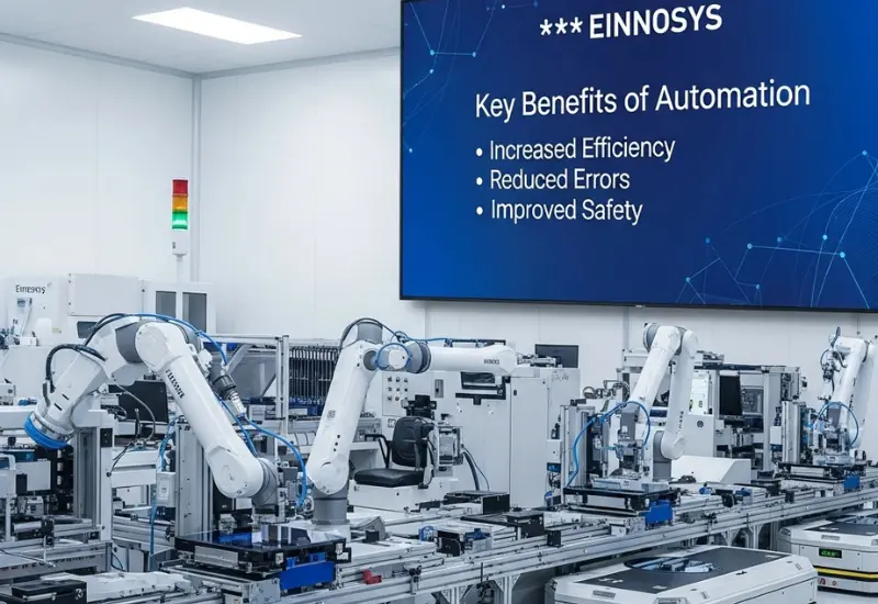
Troubleshooting an RS-232 connection often involves a breakout box (a device with LEDs showing which pins are active) and an oscilloscope. It is hardware-intensive.
Troubleshooting HSMS is done with software tools like Wireshark. An automation architecture team can capture network traffic remotely to diagnose why a tool went offline. This remote capability reduces the need for engineers to gown up and physically enter the cleanroom, saving time and reducing contamination risks.

Data Comparison: HSMS vs SECS-I

Below is a quick reference guide for semiconductor manufacturing system integrators comparing the two protocols.

Feature SECS-I (SEMI E4) HSMS (SEMI E37)

Managing the Transition in Hybrid Fabs

Unless you are building a “greenfield” fab from the ground up, you will likely encounter a mix of both protocols. This is the reality for most MES/Factory IT teams.

Strategies for Legacy Equipment

You might have a perfectly good sputtering tool from the late 90s that only speaks SECS-I. You cannot simply scrap a multi-million dollar tool because it has a slow port.

Terminal Servers: The most common solution. These devices convert RS-232 signals to Ethernet. The host talks to the terminal server via TCP/IP (often raw sockets), and the server talks to the tool via Serial. Note: This does not make the tool “HSMS.” It just allows a serial tool to live on the network.

Protocol Converters: These are smarter hardware or software boxes that actually translate SECS-I packets into HSMS messages. To the host, the old tool looks like a modern HSMS machine.

Future-Proofing New Tools

For tool OEM communication engineers, the directive is clear: Implement HSMS. Even if the current data requirements of the tool are low, customer demands will evolve. Providing an Ethernet port and a native HSMS driver ensures the tool is ready for whatever data-hungry analytics the fab decides to implement next year.

Conclusion

The battle between HSMS and SECS-I was technically won years ago, but SECS-I’s legacy remains in fabs worldwide. While SECS-I laid the groundwork for standardised automation, HSMS provided the highway necessary for the data-driven revolution of Industry 4.0. For modern Station controller designers and factory managers, HSMS is not just an option; it is a requirement for scalability, speed, and advanced control.

As you look to upgrade your facility or develop new equipment, ensure your communication layers are robust enough to handle the future. Don’t let a 30-year-old cabling standard bottleneck your million-dollar process.

FAQ

  • 1. Can I use SECS-I and HSMS on the same host system?

    Yes. Most Equipment Automation Programs (EAP) or Station Controllers are designed to handle multiple connections simultaneously. You can configure one channel to communicate via a COM port (SECS-I) and another via an IP address (HSMS) within the same application.

  • 2. Is HSMS synonymous with GEM?

    No. HSMS is the transport protocol (how data moves). GEM (SEMI E30) is the standard for equipment behaviour (what the data means). You can have HSMS without full GEM compliance, though they are usually implemented together in modern equipment.

  • 3. Does upgrading to HSMS require changing the equipment hardware?

    Usually, yes. If the tool only has a serial port, you cannot force it to speak HSMS without an intermediary PC or a protocol converter box. However, some newer controllers on older tools may have dormant Ethernet ports that can be activated with a software license upgrade.

  • 4. What is the main downside of SECS-I in a modern fab?

    Throughput. SECS-I is too slow to support detailed wafer maps, frequent trace data collection, or the rapid command/response cycles required by high-volume automated material handling systems (AMHS).

What Is the SECS/GEM Protocol? A Complete Guide to Semiconductor Automation

Introduction to SECS/GEM in Semiconductor Manufacturing

Modern semiconductor fabrication relies heavily on automation to achieve predictable processes, maximize throughput, and maintain world-class yield. Every manufacturing step—from wafer loading to deposition, etching, metrology, and packaging—depends on precise coordination between equipment and the factory’s host systems. This coordination is made possible through one of the most important communication standards in the industry: the SECS/GEM protocol.

SECS/GEM (SEMI Equipment Communications Standard / Generic Equipment Model) is the universal language that allows semiconductor tools to communicate with manufacturing execution systems (MES), factory hosts, and automation software. Without SECS/GEM, fabs would require custom communication for each tool type, making integration slow, expensive, and nearly impossible to scale.

This complete beginner’s guide explains what SECS/GEM is, how it works, and why it remains the backbone of semiconductor automation—even as the industry rapidly advances toward Industry 4.0, digital twins, and AI-driven manufacturing.

Why the SECS/GEM Protocol Matters in Modern Semiconductor Fabs

Standardizing Equipment Communication Across the Fab

Before SECS/GEM, equipment vendors each had their own proprietary communication formats. Integrating a new tool could take months of engineering work. SECS/GEM standardizes message structures, events, commands, status reporting, alarms, and behaviors so that all tools from lithography to packaging communicate uniformly.

This standardization allows fabs to:

  • Reduce integration complexity
  • Achieve faster tool qualification
  • Maintain consistent automation logic across hundreds of machines

Reducing Integration Time and Engineering Effort

Because SECS/GEM defines predictable equipment behavior, factories no longer need to build custom drivers for every tool. Integrators simply connect the equipment to the host via HSMS (Ethernet) or SECS-I (serial), configure event reports, and begin automation.

The result:

  • Shorter installation and ramp-up time
  • Lower engineering cost
  • Fewer communication-related errors

Enabling Reliable Equipment Monitoring and Control

SECS/GEM supports near real-time Equipment Monitoring, alarm reporting, and status changes, giving engineers complete visibility into production lines.
 

It also enables remote operations through standardized Remote Commands (RCMD). This makes automation scalable, safer, and more efficient.

How SECS/GEM Works: Key Components Explained

SECS Message Structure (SxFy Format)

SECS messages follow a structured format: Stream x, Function y (SxFy).
For example:

  • S1F1 — Are You There?
  • S6F11 — Event Report
  • S2F41 — Remote Command

This structured messaging ensures tools behave predictably in all factories globally.

HSMS vs SECS-I: Communication Layers and Transport Protocols

SECS-I (RS-232 serial) was the original method of communication, but most fabs today use HSMS (SEMI E37)—a high-speed Ethernet-based transport.

HSMS advantages:

  • Reliable networking
  • Higher data throughput
  • Better support for factory-wide automation

Event Reporting, Data Collection, and Alarm Handling

Key structures include:

  • Data Collection Events (DCEs)
  • Event IDs (CEIDs)
  • Status Variables (SVs)
  • Equipment Constants (ECs)
  • Alarms (ALIDs)

This rich dataset feeds into supervisory control, analytics systems, yield management tools (YMS), and AI/ML platforms.

SECS/GEM Data Analytics for Real-Time Insights

Using SECS/GEM Data for Trend Analysis and Process Stability

Fabs use SECS/GEM data to track:

  • Chamber temperature
  • Pressure stability
  • Motor torque
  • Recipe parameters
  • Wafer movement timing

Analyzing this data helps detect early process drift and maintain stability across high-volume production.

Role of SECS/GEM Data in Semiconductor Yield Optimization

Yield strongly depends on equipment health and process consistency.

SECS/GEM enables:

  • Rapid root-cause analysis
  • Correlation of equipment parameters to wafer defects
  • Faster identification of out-of-control (OOC) conditions

Yield management teams rely on clean, structured SECS/GEM data to drive consistent output quality.

Integrating SECS/GEM Data With AI/ML and Predictive Models

Modern fabs connect SECS/GEM data streams to:

  • Predictive maintenance systems
  • Fault detection and classification (FDC)
  • Machine learning-based anomaly detection

The result is fewer unexpected tool failures and significantly improved uptime.

Equipment Monitoring Through SECS/GEM

Tracking Status Variables (SVs) for Tool Health

Status Variables are real-time data points that describe machine conditions, such as:

  • Machine state
  • Substate
  • Carrier positions
  • Material handling status

These are essential for production monitoring and automated decision-making.

Using Data Collection Events (DCEs) for Performance Monitoring

DCEs trigger when key events occur—wafer load, vacuum start, recipe completion, or process errors. This allows factories to trace every part of the manufacturing process.

Alarm Management and Fault Detection

Alarms are automatically reported with:

  • Alarm ID
  • Description
  • Timestamp
  • Severity

This supports fast troubleshooting, root-cause identification, and reduced downtime.

SECS/GEM for Automation Engineers: Practical Use Cases

Remote Commands (RCMD) for Recipe and Job Control

Hosts can remotely send commands such as:

  • Start
  • Stop
  • Pause
  • Resume
  • Select Recipe

This eliminates the need for manual operator intervention.

Material Handling and Wafer Tracking Through SECS/GEM

The protocol supports automated material flow by reporting:

  • Carrier load/unload
  • Wafer count
  • Slot mapping
  • Robot errors

MES Integration and Factory Host Connectivity

SECS/GEM connects directly to:

It is the foundation of end-to-end digital manufacturing.

Comparing SECS/GEM With Other Semiconductor Communication Standards

SECS/GEM vs GEM300

GEM300 builds on SECS/GEM to support:

  • Wafer-level tracking
  • Carrier management
  • Durable handling
    Material transport automation
SECS/GEM vs SECS-II
  • SECS-II defines message structure
  • GEM defines behavior models (automation rules)

Together, they form the complete standard.

HSMS vs SECS I

Where EDA/Interface A Fits in Modern Fabs

EDA (Interface A) is used for high-frequency, high-volume data acquisition like fault detection and real-time analytics. SECS/GEM is still required for control, events, and commands.

Common Challenges When Implementing the SECS/GEM Protocol

Handling Custom Equipment Variations

Even with standardization, vendors may customize GEM implementations.
This requires careful mapping and validation.

Ensuring Robust Connection and Message Handling

HSMS sessions need reliable handling of:

  • Heartbeats
  • Reconnect logic
  • Message buffering
Maintaining Data Quality for Analytics Platforms

Poorly defined event reports or SVs degrade data analytics.
Standardized naming and timestamp accuracy are critical.

Future of SECS/GEM in Industry 4.0 Semiconductor Manufacturing

Integration With Digital Twin and AI Systems

SECS/GEM data is essential for the digital thread—from real-time digital twins to predictive process simulations.

Expanding SECS/GEM Data for Predictive Maintenance

AI-driven monitoring can detect anomalies before failures occur.

How Standards Will Evolve in Next-Gen Fabs

Future trends include:

  • Hybrid SECS/GEM + EDA architectures
  • Greater interoperability
  • Enhanced data models for robotics and automation

Conclusion

The SECS/GEM protocol is the foundation of semiconductor automation, enabling seamless communication between thousands of tools and factory systems. Even as the industry moves toward AI, real-time analytics, and hyper-automated fabs, SECS/GEM remains essential due to its reliability, consistency, and global adoption.

For beginners, mastering SECS/GEM opens doors to careers in equipment integration, automation engineering, and data-driven manufacturing—fields central to the future of semiconductor production.

FAQ Section

  • What is SECS/GEM?

    SECS/GEM is the global communication standard that connects semiconductor equipment to factory host systems.

  • Why is SECS/GEM important?

    It standardizes automation, event reporting, remote control, and data collection across fabs.

  • What does SECS stand for?

    SEMI Equipment Communications Standard.

  • What does GEM stand for?

    Generic Equipment Model.

  • What is the difference between SECS-I and HSMS?

    SECS-I uses serial communication; HSMS uses high-speed Ethernet.

  • How does SECS/GEM support equipment monitoring?

    Through status variables (SVs), alarms, and event reporting.

  • Can SECS/GEM be used for data analytics?

    Yes—SECS/GEM Data Analytics is widely used for yield improvement and predictive maintenance.

  • What is GEM300?

    An extension of SECS/GEM used for 300mm wafer automation.

  • Does SECS/GEM work with AI/ML platforms?

    Yes, SECS/GEM data is often fed into ML models for process optimization.

  • Is SECS/GEM still relevant with newer standards like EDA?

    Yes—SECS/GEM is essential for control and automation; EDA complements it for high-volume data.

EDA Semiconductor Guide: Powering Faster, Smarter Chips

Summary

  • Market Growth: The global Electronic Design Automation (EDA) market is projected to reach significant heights by 2030, driven by the demand for complex SoCs and AI chips.
  • Core Function: EDA is not merely drawing circuits; it encompasses simulation, verification, and manufacturing analysis to prevent costly silicon failures.
  • Fab Integration: Modern EDA tools bridge the gap between design and the fab floor, heavily influencing Design for Manufacturing (DFM) and yield rates.
  • Future Tech: AI and machine learning are reshaping EDA, automating floor planning and reducing design cycles from months to weeks.
  • Strategic Value: For fab managers and CTOs, integrating robust EDA workflows is essential for maintaining throughput and handling the transition to Angstrom-era nodes.

Introduction

According to a report by Grand View Research (2023), the global Electronic Design Automation (EDA) market size was valued at over $11 billion in 2022 and is expected to expand at a compound annual growth rate (CAGR) of 9.1% from 2023 to 2030. That is a lot of money spent on software just to figure out where to put transistors. But when you consider that a single cutting-edge wafer run can cost millions, spending heavily on the roadmap makes perfect sense.

Modern microchips are cities built on a fingernail. We are talking about billions of transistors packed into a space smaller than a postage stamp. Managing this level of complexity manually is impossible. It would be like trying to memorise every phone number in New York City. This is where eda semiconductor tools come in. They serve as the architect, the structural engineer, and the safety inspector for the semiconductor industry.

For the fab managers and automation engineers reading this, you know that the design phase and the manufacturing phase used to be polite strangers. They waved at each other from across the room. Now, they have to be best friends. The data flowing from eda software directly impacts equipment calibration, yield improvement, and the overall efficiency of the cleanroom.

EDA in Semiconductor Manufacturing

What is EDA in Semiconductor Manufacturing?

To the uninitiated, it looks like very complicated drawing software. But asking what is eda in semiconductor workflows is reveals a much deeper function. It is a category of software tools for designing electronic systems such as integrated circuits (ICs) and printed circuit boards (PCBs).

Beyond Just Drawing Circuits

In the early days, chip design was largely manual. Engineers used tape and Mylar sheets to lay out circuits. If you made a mistake, you grabbed an X-Acto knife. Today, EDA is about physics and logic.

The software simulates how electricity moves through metal and silicon. It predicts heat dissipation. It checks if a signal arriving at point A will get to point B before the clock cycles. It is a simulation of reality that happens long before a single photon hits a photoresist layer.

The Bridge Between Design and Fabrication

For the plant heads and OEM tool makers, EDA is the set of instructions your machines eventually receive. The output of the EDA process, usually a GDSII or OASIS file is the blueprint the scanner uses to print patterns.

If the EDA tools do not account for the physical limitations of the lithography equipment, the chip fails. This connection is why “Design for Manufacturing” (DFM) has become a buzzword that actually means something. The software has to know what the hardware can do.

The Engine of Moore’s Law:Why EDA Semiconductor Tools Matter

Moore’s Law states that the number of transistors on a microchip doubles about every two years. Keeping this law alive has become incredibly difficult. We are running up against the laws of physics, and physics is a strict negotiator.

Handling Unimaginable Complexity

Apple’s M2 Ultra chip consists of 134 billion transistors. A human brain cannot comprehend the interconnectivity required to make that work. Semiconductor eda platforms manage this complexity through abstraction.

Engineers design high-level behaviour, and the software translates that into logic gates and then into physical layouts. It automates the tedious work. Without automation, designing a modern GPU would take centuries. We don’t have that kind of time; the holiday shopping season is coming up.

Reducing “Spin” Costs

In the industry, a “spin” refers to a revision of the silicon. If you tape out a chip, manufacture it, and find a bug, you have to do a re-spin.

According to Synopsys (2023), a re-spin at advanced nodes (like 5nm or 3nm) can cost tens of millions of dollars and delay a product by 6 to 9 months. That is a career-ending mistake for a product manager. Electronic design automation software exists primarily to ensure that the chip works in the simulation so you don’t burn cash in the fab.

Key Components of Electronic Design Automation Software

The EDA ecosystem is vast, but it generally breaks down into three critical stages. Understanding these helps automation engineers see where their equipment data might eventually feed back into the design loop.

Logic Design and Synthesis

This is the “what does it do?” phase. Engineers write code in languages like Verilog or VHDL to describe the behaviour of the chip. The eda design software then takes this code and “synthesises” it.

Think of it like compiling code for a computer program, but instead of turning it into machine code, the software turns it into a netlist, a massive list of logic gates and how they connect.

Physical Design (Place and Route)

This is the “where does it go?” phase. The software takes those billions of logic gates and figures out where to place them on the silicon slice.

It simulates a game of Tetris where the pieces are microscopic, and they all generate heat. The “Route” part involves connecting these gates with copper wiring without creating short circuits or delays. This step is computationally heavy and often runs on massive server farms.

Verification and Sign-off with EDA Semiconductor Tools

Before the files go to the fab, the design undergoes a physical check.

  • DRC (Design Rule Check): Does the spacing between wires meet the foundry’s minimum requirements?
  • LVS (Layout vs. Schematic): Does the physical picture match the logical plan?

If the software says “Pass,” the design is signed off. If it says “Fail,” someone is working late.

The Intersection of EDA Software and Factory Automation

Here is where Einnosys enters the chat. For a long time, EDA was an island. Now, Industry 4.0 is building bridges to that island.

Closing the Loop with Yield Data

Fabs generate terabytes of data daily via SECS/GEM and other protocols. Smart factories are now taking yield data information on where and why chips are failing and feeding it back into the eda semiconductor environment.

If a specific layout pattern consistently causes defects in the Etch or Deposition chambers, the EDA tools can be updated to flag that pattern as “risky” in future designs. This creates a learning loop. The factory teaches the design software how to be better.

Design for Manufacturing (DFM)

DFM is the art of modifying a design to make it easier to build. It involves:

  • Adding redundant vias to ensure connections.
  • Adjusting wire widths to account for lithography variance.

Automation engineers and equipment makers play a role here. The capabilities of the toolset define the DFM rules. If your new Etcher has better precision, you can update the DFM rules in the eda software to allow for tighter packing, getting more chips per wafer.

Future Trends in Semiconductor EDA

The industry never sleeps. As we move toward 2nm nodes and Angstrom-era computing, the tools are evolving.

AI and Machine Learning in Design

Artificial Intelligence is designing chips for Artificial Intelligence. It is very meta. According to a report by Deloitte (2023), top semiconductor companies are using AI within their EDA tools to optimise floor planning.

AI can explore millions of potential layouts in hours a task that would take a team of human engineers weeks. It finds efficiencies that humans miss, reducing power consumption and silicon area.

Chiplets and Advanced Packaging

We are hitting the size limit of what we can print on a single die (the reticle limit). The solution is Chiplets, stacking smaller dies together like Lego bricks.

This requires a new breed of eda design software that handles 3D structures. The tools must analyse heat and electrical current flowing vertically between stacked chips, not just horizontally.

Conclusion

The race for smaller, faster, and more energy-efficient electronics is relentless. At the heart of this race sits eda semiconductor technology. It is the translator that turns human ingenuity into silicon reality.

For fab managers, equipment engineers, and R&D teams, the goal is clear: tighter integration. The future belongs to those who can connect the digital design world with the physical manufacturing floor. Whether it is through better SECS/GEM implementation, smarter yield analysis, or AI-driven workflows, the tools are there to be used.

Frequently Asked Questions

  • How does EDA software impact yield in a semiconductor fab?

    EDA software includes Design for Manufacturing (DFM) tools that identify potential printing errors before the design hits the fab. By adhering to strict foundry rules during the design phase, the software ensures that the patterns can be successfully reproduced by the lithography equipment, directly increasing the number of functional chips per wafer.

  • Can AI replace human engineers in EDA?

    Not entirely. AI is excellent at optimisation and handling repetitive tasks like routing wires or placing blocks to minimise heat. However, the high-level architecture and creative logic design still require human intuition. AI acts more like a super-powered assistant that speeds up the process rather than a replacement.

  • What is the difference between CAD and EDA?

    CAD (Computer-Aided Design) is a broad term often used for mechanical 3D modelling (like designing a car part). EDA is a specific subset of CAD tailored for electronics. It deals with electrical properties, circuit logic, and silicon physics, which standard mechanical CAD tools do not handle.

  • Why is cloud computing becoming important for EDA?

    Modern chip designs are massive. Running the necessary simulations and physical verifications requires immense processing power. Cloud computing allows companies to burst their compute capacity, renting thousands of cores for a few hours to run a check, rather than maintaining expensive internal data centres that sit idle half the time.