반도체 공장 자동화: 주요 장점 및 Einnosys 솔루션

요약

  • 통계적 성장: 전 세계 반도체 매출은 2024년 6,260억 달러로 전년 대비 18.1% 증가하며 팹 인프라 투자를 가속화하고 있습니다(Gartner, 2025).
  • 효율 향상: 자동화 도입 시 생산 현장 처리량이 20~30% 증가하고 단위 생산 비용이 20% 절감될 수 있습니다(McKinsey, 2023).
  • Einnosys 효과: EIGEMBox 및 SeerSight 솔루션은 연간 200만 달러 이상의 다운타임 절감과 팹당 5,000개 이상의 웨이퍼 스크랩 방지를 지원합니다(Einnosys, 2025).
  • 미래 전망: AI 칩 수요 증가로 인해 2025~2027년 사이 300mm 팹 장비 투자가 4,000억 달러에 이를 것으로 예상됩니다(SEMI, 2024).

소개

Gartner(2025) 자료에 따르면 2024년 전 세계 반도체 매출은 6,260억 달러로 전년 대비 18.1% 증가했습니다.
이 성장은 단순히 “더 많은 칩 판매”가 아니라, 거의 무결한 제조 품질에 대한 압박이 극도로 증가하고 있음을 의미합니다.

노드 크기 축소와 AI 칩 수요 폭증으로 인해 현대 팹 운영 복잡성은 인간이 감당할 수 있는 범위를 넘어섰습니다.
이 때문에 공장 자동화는 단순한 경쟁 우위가 아니라 생존을 위한 필수 요소로 자리 잡고 있습니다.

자동화는 수천 개의 공정을 실시간으로 조율하는 디지털 신경망으로 작동하며, 미세한 진동이나 먼지 한 입자로 인해 수백만 달러 규모의 웨이퍼 배치를 폐기하는 상황을 방지합니다.

궁극적으로 엔지니어와 팹 관리자에게 중요한 목표는 다음 두 가지입니다:

  • 처리량 극대화
  • 폐기 최소화

이제 자동화가 혼란스러운 생산 라인을 어떻게 정밀하고 데이터 기반의 체계로 탈바꿈시키는지 살펴보겠습니다.

팹 자동화로의 전략적 전환

자동화의 목적은 인간을 대체하는 것이 아니라, 인간이 가진 변동성과 불확실성으로부터 공정을 보호하는 것입니다.
반도체 제조에서 일관성은 절대적인 가치입니다.

수동 작업, 종이 기반 운영 방식은 이미 시대에 맞지 않습니다.
현대 팹의 핵심은 장비 레벨부터 MES(제조 실행 시스템)까지 이어지는 엔드 투 엔드 데이터 연동입니다.

운영 효율(OEE) 향상

공장 자동화의 가장 빠른 효과는 OEE(설비 종합 효율) 향상입니다.

연구에 따르면 자동화 기반 생산 혁신은:

  • 처리량 20~30% 증가
  • 단위 생산 비용 20% 절감

이라는 결과를 가져올 수 있습니다.

이는 단순한 퍼포먼스 개선이 아니라,
분기 출하 목표 달성 여부를 결정하는 핵심 요소가 됩니다.

글로벌 인력 부족 해결

반도체 산업은 다음과 같은 문제에 직면해 있습니다:

  • 칩 수요는 증가
  • 숙련 인력은 감소

현대 자동화 시스템은 수동, 반복적인 웨이퍼 운송과 로딩 작업을 대신 수행하여,
엔지니어들이 **고부가가치 업무(수율 분석, 공정 최적화)**에 집중할 수 있게 합니다.

참고:
로봇이 심심함을 느끼는지 모르겠지만,
숙련 엔지니어가 매번 알람을 수동 기록해야 한다면 그건 정말 지루한 일입니다.

공장 자동화 장비의 핵심 이점

공장 자동화 장비 투자는 초기 비용이 크지만, 그 효과는 팹 운영 전반에 걸쳐 나타납니다.

향상된 수율 및 스크랩 감소

수율은 팹의 최종 성적표입니다.
단 한 번의 처리 오류도 수만 달러짜리 웨이퍼를 폐기하게 만들 수 있습니다.

자동화는 인적 접촉을 최소화하여:

  • 오염 감소
  • 물리적 손상 감소
  • 웨이퍼 스크랩 감소

와 같은 효과를 제공합니다.

Einnosys는 연간 5,000개 이상의 웨이퍼 불량을 방지한다고 보고합니다.

실시간 데이터 가시성 확보

많은 구형 팹은 다음과 같은 문제를 겪습니다:

  • 장비가 데이터를 생성하지만
  • 시스템이 이를 수집하지 못하고 분석도 못함

즉, “보이지 않는 데이터(dark data)”입니다.

현대 자동화 시스템은:

  • 장비 상태
  • 가스 흐름
  • 온도 변화

등을 실시간으로 시각화하여 예측 유지보수 체계를 구축합니다.

Einnosys 반도체 현장 맞춤 자동화 기술 선도

Einnosys는 일반적인 자동화 장비가 아니라
반도체 팹의 특수 요구사항(예: SECS/GEM, 레거시 장비 통합)을 해결하는
전문화된 자동화 솔루션을 제공합니다.

EIGEMBox  레거시 장비의 한계를 해결

많은 팹이 200mm 구형 장비를 여전히 사용하고 있습니다.
문제는 이 장비들이 현대적 통신 기능이 없다는 점입니다.

EIGEMBox는:

  • 기존 장비 전체 교체 없이
  • SECS/GEM 기능을 추가

하는 특허 기술 솔루션입니다.

레거시 팹이 데이터 기반 생산 체계에 합류할 수 있도록 돕습니다.

SeerSight & xPump 기반 예측 인텔리전스

다운타임은 팹 운영에서 가장 큰 비용입니다.

Einnosys의 SeerSight 및 xPump는:

  • AI/ML 기반 분석
  • 펌프 및 공정 상태 실시간 감지
  • 고장 수주 전 사전 경고

를 제공하여 연간 200만 달러 이상의 다운타임 비용을 절감할 수 있습니다.

비용 vs 역량 — 자동화의 경제적 현실

자동화는 비싸지만,
운영 실패보다 훨씬 저렴합니다.

2025년 300mm 팹 장비 투자액은
역대 최초로 1,000억 달러를 돌파할 전망입니다.

이는 AI 기반 반도체 시장의 폭발적 성장 때문입니다.

기능 비교표

항목 수동/레거시 방식 자동화 스마트 팹
처리량 교대 근무에 제한됨 24시간 연속 운영
오류율 사람 요인에 따라 변동 일관적이며 프로그램 기반
유지보수 고장 후 대응 예측 유지보수
확장성 인력 증가에 의존 디지털 기반 확장

인더스트리 4.0 준비

스마트 팩토리 구현은 단순히 로봇을 구매하는 것이 아닙니다.
팩토리 IT 아키텍처의 역할 재정의가 핵심입니다.

장비에서 발생한 데이터가 몇 시간 후가 아니라 몇 초 만에
AI 기반 수율 모델로 전달될 수 있어야 합니다.

표준 프로토콜(SECS/GEM)이 없다면,
자동화 장비는 “아무 말도 못하는 빠른 기계”일 뿐입니다.

팹 현대화의 미래 트렌드

2028년을 향한 핵심 흐름:

  • 2nm 이하 초미세 공정: 인간이 감독 불가한 원자 단위 정밀도 요구
  • 글로벌 지역화: 미국·유럽·인도 등 신규 팹 확산
  • 지속 가능성: 에너지·용수 절감 자동화 필요

결론

반도체 산업에서 성공하려면
데이터·정밀성·자동화가 필수입니다.

Einnosys와 같은 전문 파트너는
완전 자동화 팹 실현을 앞당기는 핵심 역할을 하고 있습니다.

Contact Us Today

반도체 공장 자동화를 단계별로 지원받으세요


Boost Semiconductor Factory Efficiency with Automation Software

Summary

  • Modern semiconductor manufacturing demands extreme precision that manual processes fail to provide.
  • Implementing semiconductor factory automation software can reduce operational costs by up to 20% while increasing throughput (McKinsey, 2023).
  • Key technologies include SECS/GEM protocols, advanced MES integration, and AI-driven predictive maintenance.
  • Automation minimizes human error in cleanroom environments, protecting delicate silicon wafers from contamination.
  • The transition toward “Lights Out” manufacturing is a competitive necessity for 300mm fabs.

Introduction

According to McKinsey & Company (2023), AI and advanced analytics integrated into semiconductor factory automation software can reduce manufacturing costs by 15% to 20% for established fabs. This shift is essential as global demand for chips fluctuates, forcing facilities to find every possible margin for improvement. Efficiency is no longer a goal; it is a requirement for survival in a market where a single speck of dust or a millisecond of lag can ruin a million-dollar batch.

High-volume manufacturing requires a delicate balance of chemical precision, mechanical speed, and digital oversight. The introduction of robust fab automation solutions allows managers to oversee these complexities without constant manual intervention. By digitizing the workflow, companies ensure that every tool in the facility operates at its theoretical limit.

The current landscape of chip production is becoming more crowded and expensive. New facilities often cost upwards of $20 billion, making the software that runs them as valuable as the hardware itself. Adopting semiconductor factory automation software provides the backbone for these massive investments, ensuring that the return on investment remains high even as nodes shrink toward the sub-2nm frontier.

Why Software Defines the Modern Fab

Modern semiconductor manufacturing is less about the physical act of etching silicon and more about the data governing those etches. Human operators are remarkably talented, yet they are also walking biological contamination factories. A single skin cell can terminate a wafer’s journey. Automation software moves the human element away from the delicate front-end processes, placing them in control rooms where they can make strategic decisions rather than manual adjustments.

Eliminating the Human Variable

Does anyone actually miss the days of tracking wafer lots with physical clipboards and pens? Moving to a fully digital environment removes the risk of “fat-finger” errors where a technician might accidentally input the wrong recipe for a photolithography step. Software systems enforce strict compliance, ensuring that a tool will refuse to start unless the parameters match the pre-approved recipe perfectly.

Maximizing Equipment Effectiveness

High-end tools like EUV lithography machines are too expensive to sit idle. Industrial automation software tracks Equipment Health Rating (EHR) and Overall Equipment Effectiveness (OEE) in real-time. If a tool begins to drift from its baseline, the software triggers an alert before the tool fails. This proactive approach changes maintenance from a reactive headache into a scheduled, predictable task.

Core Components of Semiconductor Factory Automation Software

A comprehensive software suite acts as the nervous system for a production facility. It connects the “brains” (the planning systems) to the “muscles” (the robotic arms and process tools). Without a unified layer of semiconductor factory automation software, a fab is simply a collection of expensive machines that speak different languages.

MES Software for Semiconductors

The Manufacturing Execution System (MES) serves as the central hub for all production activities. It tracks every wafer from the moment it enters the fab as a blank slate until it leaves as a finished die. MES software for semiconductors manages lot genealogy, ensuring that if a defect is found later, the team can trace it back to a specific tool or chemical batch.

Inventory and Material Handling

The movement of Front Opening Unified Pods (FOUPs) is a logistical puzzle. Automated Material Handling Systems (AMHS) rely on software to prioritize specific lots. If a high-priority customer order needs to jump the queue, the software reroutes the FOUPs across the ceiling-mounted tracks without causing a traffic jam in the cleanroom.

SECS/GEM and Connectivity

Communication protocols like SECS/GEM allow the software to talk to tools from different vendors. This standardization is what makes fab automation solutions viable. It creates a universal translator so that a South Korean etch tool and a Dutch lithography machine can both report their status to a centralized server in the United States.

Achieving Semiconductor Process Optimization

Efficiency is a game of inches or in this case, nanometers. Semiconductor process optimization involves analyzing thousands of data points per second to find bottlenecks. When software identifies that a specific chemical mechanical planarization (CMP) tool is taking 5% longer than its peers, engineers can intervene before that delay ripples through the entire line.

Real-Time Data Visualization

Data is useless if it stays buried in a database. Modern software provides dashboards that allow fab managers to see the status of the entire floor at a glance. Visualizing these workflows makes it obvious where wafers are stacking up. Often, a simple software tweak to the scheduling algorithm can clear a bottleneck that appeared to be a hardware limitation.

Digital Twins and Simulation

Some automation suites now offer “Digital Twin” capabilities. This allows engineers to test a new process recipe in a virtual environment before applying it to physical silicon. Testing in a sandbox environment prevents costly mistakes and speeds up the time-to-market for new chip designs.

The Role of AI in Industrial Automation Software

Artificial Intelligence is moving past the “hype” phase and into the practical phase. In the context of industrial automation software, AI acts as a 24/7 supervisor that never sleeps or needs a coffee break. It looks for patterns that are too subtle for a human eye to detect, such as a microscopic vibration in a robotic arm that precedes a total failure by three days.

Predictive vs. Preventive Maintenance

Preventive maintenance is like changing your car’s oil every 5,000 miles, regardless of how you drive. Predictive maintenance is like the car telling you exactly when the oil is dirty. By using semiconductor factory automation software with AI, fabs avoid replacing perfectly good parts, which saves money and reduces tool downtime.

Yield Enhancement via Machine Learning

Machine learning models analyze yield maps to find the “signature” of specific faults. If a cluster of dead chips appears on the edge of every wafer, the AI can correlate that pattern with a specific cooling vent in a furnace. This level of insight would take a human engineer weeks to find; the software does it in minutes.

Navigating the Challenges of Implementation

Switching to a new software architecture is a bit like performing heart surgery while the patient is running a marathon. Fabs cannot simply stop production for a month to install new code. The process must be incremental.

  • Legacy Tool Support: Older tools might lack the sensors required for modern data collection.
  • Data Silos: Different departments often use different software, making it hard to get a “single source of truth.”
  • Cybersecurity: As fabs become more connected, they become bigger targets for industrial espionage.
  • Skill Gaps: Automation requires a workforce that is as comfortable with Python as they are with physics.

Despite these hurdles, the cost of staying manual is far higher than the cost of upgrading. A fab that fails to automate will eventually find itself unable to compete with the yields and pricing of “Lights Out” facilities.

Future Trends in Semiconductor Automation

The industry is currently looking toward “Autonomous Labs” and edge computing. As we move closer to the physical limits of silicon, the software must become more autonomous. We are seeing a move toward decentralized control, where individual tools make localized decisions to optimize their own performance without waiting for a command from the central MES.

Visualizing a fab where the machines “negotiate” with each other for priority might sound like science fiction, but it is the logical conclusion of current trends. If an etch tool knows it has a filter change coming up, it can signal the lithography tool to slow down slightly to prevent a pile-up. This level of harmony is the ultimate goal of semiconductor factory automation software.

Conclusion

The complexity of modern chipmaking has surpassed the capacity of manual oversight. Facilities that embrace semiconductor factory automation software gain a massive advantage in yield, speed, and cost-efficiency. By integrating MES, AI, and standardized communication protocols, manufacturers can turn their facilities into highly tuned, data-driven engines of production. If you want to keep your fab competitive in an era of shrinking nodes and rising costs, the software is your most important tool.

Contact Us Today

Get Professional Support to Optimize Production and Reduce Downtime


Revolutionizing Semiconductor Manufacturing with Automation Technologies

Summary

  • Efficiency Gains: Automation increases fab throughput by removing human error and optimizing material transport.
  • Yield Improvements: Advanced sensors and AI-driven analytics detect defects earlier than manual inspections.
  • Market Growth: The push toward 2nm and 3nm nodes makes semiconductor manufacturing automation a necessity rather than a luxury.
  • Data Integration: Modern fab automation solutions rely on SECS/GEM protocols for seamless equipment-to-host communication.
  • Future Readiness: Transitioning to “lights-out” manufacturing reduces contamination risks and operational overhead.

Introduction

According to a report by McKinsey & Company (2022), the global semiconductor industry is on track to become a $1 trillion sector by 2030. This massive expansion places unprecedented pressure on fabrication plants to increase output while maintaining microscopic precision. To meet these demands, semiconductor manufacturing automation has shifted from a peripheral upgrade to the central nervous system of the modern fab.

The complexity of contemporary chip design means a single mistake during the photolithography or etching stage can lead to millions of dollars in scrapped material. Automation acts as a safeguard, ensuring that every movement within the cleanroom is executed with robotic consistency. Beyond simple robotics, the integration of smart software allows for real-time adjustments that humans simply cannot perform at scale.

Facilities that embrace industrial automation in semiconductor environments see a drastic reduction in cycle times. By removing the variability of manual handling, these plants achieve higher reliability and a more predictable supply chain. As the industry moves toward increasingly smaller nodes, the margin for error disappears, making automated systems the primary driver of competitive advantage.

The Evolution of Semiconductor Process Optimization

The journey from manual wafer handling to fully autonomous environments marks a significant era in electronics history. In the early days, technicians moved wafers by hand, a process that invited contamination and physical damage. Today, the focus has shifted toward semiconductor process optimization through sophisticated material handling and data-driven decision-making.

Moving Beyond Manual Handling

Modern fabs utilize Automated Material Handling Systems (AMHS) to transport wafers between process steps. These systems, often involving Overhead Hoist Transport (OHT) or Automated Guided Vehicles (AGVs), minimize the vibration and particles that human operators inevitably introduce. Because a single speck of dust can ruin a 300mm wafer, keeping humans away from the product is a primary goal.

The Impact of 300mm and 450mm Wafers

As wafer sizes increased, their weight and fragility made manual transport nearly impossible. Automation became the solution for handling these heavy loads without sacrificing speed. This transition required a complete redesign of fab layouts to accommodate tracks, elevators, and robotic arms that operate in tight spaces.

Key Technologies in Fab Automation Solutions

Implementing effective fab automation solutions involves a mix of hardware and software working in tandem. It starts with the equipment on the floor and extends to the cloud-based analytics that predict when a machine might fail.

Equipment Communication and SECS/GEM Protocols

For a tool to be “automated,” it must communicate with the Manufacturing Execution System (MES). This is achieved through SECS/GEM (Semiconductor Equipment Communication Standard/Generic Equipment Model). These protocols allow the factory host to start or stop processing, track wafer locations, and collect data for quality control.

The Role of E58 and E142 Standards

Beyond basic communication, standards like SEMI E58 (Object Management) and E142 (Substrate Mapping) provide deeper insights. They help engineers track the “genealogy” of a chip. If a defect appears in the final testing phase, automation software can trace it back to the exact chamber and time of the incident.

AI and Machine Learning in Defect Detection

Visual inspection used to be a bottleneck. Today, high-speed cameras paired with machine learning algorithms scan wafers for imperfections at speeds no human could match. These systems learn from every scan, becoming more accurate over time and reducing “false catches” that slow down production.

Strategic Benefits of Industrial Automation in Semiconductor Fabs

Why do stakeholders invest billions in these systems? The ROI comes from three main areas: yield, throughput, and safety. A silicon wafer is essentially a very expensive piece of glass that refuses to cooperate if the environment is slightly off. Automation ensures that the environment remains perfect.

  • Yield Enhancement: Automated metrology identifies process drifts before they result in scrapped wafers.
  • Reduced Contamination: Fewer humans in the cleanroom means fewer skin cells and fibers entering the airflow.
  • Lower Operational Costs: While initial CAPEX is high, the long-term cost per wafer drops as throughput increases.
  • Safety Improvements: Robotic systems handle hazardous chemicals and heavy machinery, protecting the workforce from workplace accidents.

Overcoming Challenges in Semiconductor Manufacturing Automation

Despite the benefits, the road to a fully automated fab is paved with technical hurdles. Legacy equipment remains one of the largest obstacles for established companies. Older machines frequently lack the native digital interfaces required for modern manufacturing technology in semiconductors.

Integrating Legacy Tools

Many fabs operate with “vintage” tools that are still mechanically sound but digitally silent. Engineers often use “retrofitting” to add sensors and communication bridges to these machines. This allows a 20-year-old etcher to participate in a modern data ecosystem without requiring a multi-million-dollar replacement.

Data Silos and Interoperability

Even with new equipment, data often gets trapped in proprietary formats. True semiconductor manufacturing automation requires a horizontal data flow where the lithography tool “talks” to the development track. Breaking these silos is a major focus for MES engineers who want a holistic view of the factory floor.

The Future of Lights-Out Manufacturing

The “lights-out” factory is the ultimate goal for many high-volume manufacturers. In this scenario, the fab operates with zero human intervention on the production floor. This setup relies on advanced AI to manage scheduling and maintenance autonomously.

Digital Twins and Predictive Maintenance

Digital twins are virtual replicas of the physical fab. By running simulations on a digital twin, engineers can predict how a change in the production schedule will affect throughput. This prevents “bottlenecking” before it occurs in the real world. Predictive maintenance takes this further by analyzing vibration and heat data to schedule repairs before a tool breaks down.

Workforce Shift: From Operators to Orchestrators

Automation fails to eliminate jobs; instead, it changes their nature. The role of a fab worker is evolving from manual labor to system orchestration. Engineers now focus on optimizing algorithms and managing robotic fleets rather than moving boxes. Is your team ready to trade their wrenches for code? This shift requires significant upskilling and a new approach to technical training.

Implementing Manufacturing Technology in Semiconductors

Selecting the right partner for automation is a critical decision. It involves evaluating the scalability of software and the durability of hardware. A successful implementation usually follows a phased approach to avoid disrupting current production.

  1. Assessment: Identify the biggest bottlenecks in the current workflow.
  2. Pilot Programs: Automate a single line or process step to prove ROI.
  3. Data Harmonization: Ensure all tools speak a common language (SECS/GEM).
  4. Full Integration: Connect the floor tools to the MES and ERP systems.
  5. Continuous Optimization: Use AI to refine processes based on real-time data.

Conclusion

The transition toward semiconductor manufacturing automation is no longer a choice for those who wish to remain relevant. With global demand for chips skyrocketing and transistor sizes shrinking to the atomic level, the precision of robotics and the speed of AI are the new industry standards. By investing in fab automation solutions, manufacturers can ensure higher yields, lower costs, and a safer environment for their workforce.

Contact Us Today

Get Expert Help to Implement Advanced Fab Automation Technologies


How GEM300 Enables 300mm Semiconductor Factory Automation

Summary

  • The 300mm Paradigm: Examining how the transition from 200mm to 300mm wafers necessitated the shift toward fully automated software control.
  • Core SEMI Standards: A technical breakdown of E87 (Carrier Management), E40 (Process Jobs), E94 (Control Jobs), and E90 (Substrate Tracking).
  • Performance Metrics: How compliance directly improves Overall Equipment Effectiveness (OEE) and reduces scrapped material.
  • OEM Strategy: Guidelines for equipment manufacturers to achieve seamless integration with factory host systems.
  • Future Resilience: The role of automation in supporting “lights-out” manufacturing and AI-driven process control.

Introduction

According to Statista (2024), 65% of global semiconductor manufacturing capacity expansion is now focused exclusively on 300mm facilities, with total monthly capacity expected to hit 9.6 million wafers by 2026. This massive investment underscores a critical reality in modern electronics: the era of manual intervention is over. To manage these gargantuan volumes with the precision of a master watchmaker, the industry relies on a sophisticated framework known as GEM300 factory automation.

When the industry moved from 200mm to 300mm wafers, the changes were far more than just physical. A fully loaded 300mm Front Opening Unified Pod (FOUP) weighs roughly 9 kilograms and carries silicon worth as much as a luxury sports car. Expecting a human technician to carry these across a cleanroom floor is a recipe for both ergonomic disasters and financial heartbreak. Silicon is quite the diva; it demands a vibration-free, perfectly clean, and highly predictable environment to yield results.

To solve this, the industry standardized the communication between the factory host and the equipment. This standardization ensures that every tool in a 300mm semiconductor fab speaks the same digital dialect. Without these rules, a factory would be a chaotic Babel of proprietary software, where the robots and the process tools could never agree on when to start or stop. GEM300 factory automation provides the script that keeps the entire facility in sync.

The Physical Necessity of 300mm Semiconductor Fab Automation

In older 200mm fabs, automation was often a luxury or a secondary thought. Operators could manually move “open cassettes” and use basic barcode scanners to tell the host which lot was being processed. In a 300mm environment, however, the wafers are housed in sealed FOUPs to maintain a pristine micro-environment. This makes manual identification and handling virtually impossible at scale.

The sheer size of these wafers also means that the cost of a single error is magnified. If a batch of wafers is processed with the wrong recipe, the financial loss is roughly 2.25 times higher than it was in the 200mm era. Automation isn’t about saving on labor costs; it’s about eliminating the variance that humans inherently introduce into a system.

The Evolution from SECS/GEM to GEM300

While the original SECS/GEM (E30) standards provided a way for tools to report their status, they were designed for simpler times. Basic GEM can tell a host that a tool is “Running” or “Idle,” but it lacks the nuance required to handle automated overhead transport systems or complex job queuing. GEM300 factory automation was developed to fill these gaps, providing a comprehensive management layer for material, recipes, and substrate locations.

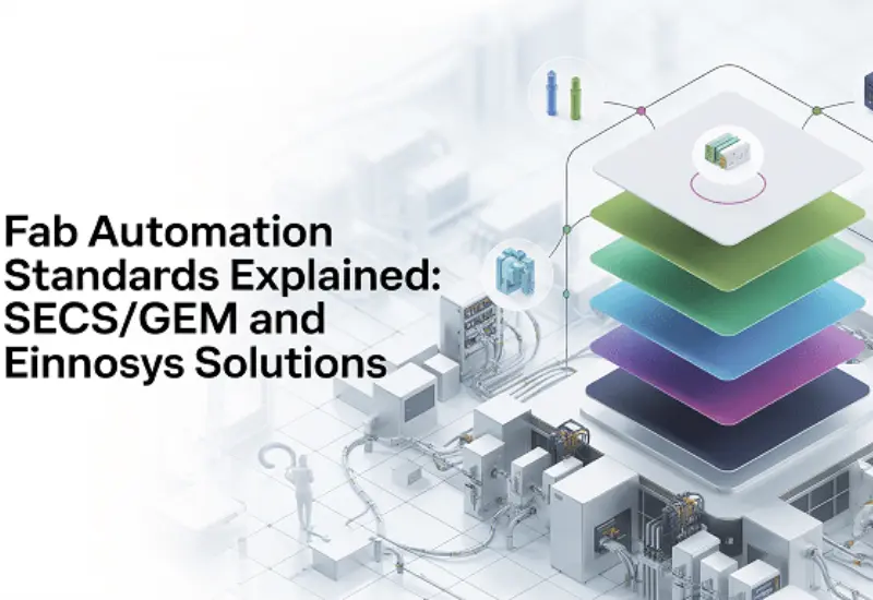
Deciphering the Core SEMI GEM 300 Standards

The term SEMI GEM 300 refers to a suite of standards that work together to create a “hands-off” manufacturing environment. Each standard addresses a specific logistical challenge.

E87 – Carrier Management System (CMS)

E87 is perhaps the most visible part of the automation suite. It manages the interaction between the equipment and the material carriers (FOUPs).

  • Load Port Control: It manages the state of the load ports, signaling to the Overhead Hoist Transport (OHT) when a port is ready for a new pod.
  • Carrier ID Verification: It ensures that the ID of the FOUP matches the ID expected by the factory host.
  • Content Map: E87 checks that the number of wafers reported by the pod’s sensor matches the factory records.

E40 – Process Job Management

A Process Job is the digital instruction that tells a tool what to do with a specific set of wafers. It specifies the recipe to be used and the specific wafers within the FOUP that should be processed. E40 allows the factory host to download these instructions in advance, ensuring the tool is ready to start the moment the FOUP is clamped and unsealed.

E94 – Control Job Management

If the Process Job is the “what,” the Control Job is the “how and when.” E94 organizes multiple process jobs into a logical sequence. It manages the flow of material through the tool, coordinating how different carriers are handled if a tool has multiple load ports. This allows for continuous processing, where the tool is already preparing for the next batch while the current one is still in the process chamber.

E90 – Substrate Tracking

In high-end chipmaking, knowing where a wafer is isn’t enough; you need to know exactly which slot it occupies at every microsecond. E90 provides real-time tracking of every individual wafer (substrate) as it moves from the FOUP to the robot arm, into the load lock, and through the process modules. This is essential for modern “wafer-level traceability.”

Operational Gains through GEM300 Factory Automation

Why do companies spend millions on GEM300 compliance? The answer lies in the data. According to a McKinsey (2023) report on semiconductor manufacturing, fabs that implement high-level automation see an average increase of 15% in Overall Equipment Effectiveness (OEE).

Eliminating the “Fat Finger” Error

Manual data entry is the enemy of yield. When an operator has to type in a recipe name like “ETCH_GATE_POLY_V2,” there is a constant risk of a typo. Semiconductor equipment automation removes this risk. The host system sends the recipe name directly to the tool via the E40 standard. The tool then verifies that it actually possesses that recipe before it even begins to move a wafer.

Reducing Cycle Times

In a manual fab, a tool might sit idle for twenty minutes while an operator realizes a process is finished and comes to move the material. In a 300mm semiconductor fab using GEM300, the tool alerts the AMHS (Automated Material Handling System) minutes before the process ends. The robot is often waiting at the load port the moment the FOUP is ready to be moved, shaving hours off the total cycle time for a single lot.

The Roadmap to GEM300 Compliance for OEMs

For Equipment Original Equipment Manufacturers (OEMs), building a tool for the 300mm market is a daunting task. You could have the most advanced etch chemistry on the planet, but if your tool cannot pass a GEM300 compliance test, no tier-one fab will buy it.

Mapping the State Machines

The biggest challenge in compliance is mapping the tool’s internal hardware states to the SEMI-defined state models. SEMI standards require the tool to report its status in a very specific way. If the tool is in a “Maintenance” state, it must report that via the software interface so the host doesn’t try to send it new work.

Handling Exception Scenarios

True automation is easy when everything goes right. It becomes difficult when things go wrong. What happens if the power blips? What if a wafer breaks inside a chamber? A SEMI GEM 300-compliant tool must be able to report these errors clearly to the host, allowing for “graceful” recovery rather than a total system crash that requires a manual reboot.

Utilizing Middleware for Faster Integration

Many OEMs choose to use specialized middleware to handle the communication layer. This allows their internal software teams to focus on the tool’s core process (like lithography or deposition) while the middleware handles the complex handshake protocols required by the smart factory SEMI standards.

The Data Layer of the Smart Factory

Modern fabs are essentially giant data centers that happen to produce silicon. GEM300 factory automation provides the primary pipeline for this data. Every event—every wafer move, every temperature change, every vacuum pressure reading—is reported through the GEM interface.

Advanced Process Control (APC)

With the rich data provided by GEM300, fabs can implement Advanced Process Control. If a metrology tool detects that a layer is slightly too thick, it can send a signal through the host to the next process tool to adjust its etch time accordingly. This “closed-loop” manufacturing is only possible because of the standardized communication provided by the GEM300 suite.

Predictive Maintenance and SVIDs

Through the use of Status Variable IDs (SVIDs), a tool can report its internal health metrics. Is the pump drawing more current than usual? Is the robot arm moving slightly slower? By analyzing this data over time, fab engineers can predict when a part is failing and schedule maintenance before the tool breaks down. This shift from “fix it when it’s broken” to “fix it before it breaks” is a massive driver of profitability.

Overcoming Challenges in Automation Implementation

Is the road to a fully automated fab paved with silicon? Yes, but it also has its share of potholes. Even with standards in place, integration can be tricky.

Variation in Fab Interpretations

While SEMI provides the “alphabet,” each fab operator often has their own “dialect.” One company might require specific custom reports that another does not. This means MES integration engineers must often customize the communication layer for every specific factory site, even if the tool is theoretically “compliant.”

Data Overload

A single tool can generate thousands of events per second. In a fab with hundreds of tools, the sheer volume of data can overwhelm older host systems. Modern smart factory SEMI standards are increasingly looking at ways to filter this data at the “edge,” ensuring that only the most critical information is sent to the central host, while the rest is stored locally for deep-dive analysis.

Conclusion

The success of modern semiconductor manufacturing depends on the seamless execution of GEM300 factory automation. By bridging the gap between physical material handling and digital process control, these standards have allowed the industry to scale to the massive volumes required by the global AI and mobile economies. As we look toward the future of 450mm wafers or even more complex 3-D chip architectures, the lessons learned from the SEMI GEM 300 transition will remain the blueprint for industrial excellence.

Contact Us Today

Get Expert Guidance to Achieve Full GEM300 Factory Automation

Fab 자동화 표준 해설: SECS/GEM 및 EINNOSYS 솔루션

요약

  • 현대 반도체 제조는 높은 수율과 최소한의 다운타임을 유지하기 위해 표준화된 통신에 의존합니다. 
  • SECS/GEM 팹 자동화는 장비와 호스트 시스템 간의 범용 언어로 작동합니다. 
  • E4, E5, E30, E37과 같은 SEMI 표준을 구현하면 원활한 데이터 교환 및 원격 장비 제어가 보장됩니다.
  •  EINNOSYS는 OEM 및 팹을 위해 복잡한 프로토콜 배포를 간소화하는 전문 소프트웨어 및 통합 서비스를 제공합니다. 
  • 이러한 표준을 채택하면 반도체 산업에서 스마트 제조 및 Industry 4.0 대비가 촉진됩니다.

서론

Statista(2024)에 따르면, 전 세계 반도체 산업 매출은 올해 약 6,130억 달러에 이를 것으로 예상됩니다. 이와 같은 막대한 재무적 규모는 제조 환경 내에서 극도의 정밀성을 요구합니다. 장비가 공장의 “두뇌”와 통신할 수 있는 통합된 방식이 없다면, 생산은 즉시 중단될 것입니다. 바로 이 지점에서 SECS/GEM 팹 자동화가 모든 설비의 주요 번역자로서 핵심적인 역할을 수행합니다.

수백만 달러에 달하는 노광 장비가 “작업 완료”라고 말하기 위해 특정 프로토콜이 왜 필요할까요? 단 하나의 먼지 입자나 몇 밀리초의 지연이 웨이퍼 배치를 망칠 수 있는 환경에서는 명확한 통신이 모든 것을 좌우합니다. 표준화된 프로토콜은 서로 다른 장비들이 하나의 통합된 시스템처럼 동작할 수 있도록 합니다. 이러한 표준이 없다면, 엔지니어들은 실제 칩 생산보다 맞춤형 드라이버 작성에 더 많은 시간을 소비하게 될 것입니다.

현대적인 팹을 구축하는 것은 고급 하드웨어만으로는 충분하지 않습니다. 실시간 모니터링 및 제어를 가능하게 하는 반도체 자동화 표준의 견고한 프레임워크가 필수적입니다. 본 문서는 이러한 프로토콜이 어떻게 작동하는지, 그리고 EINNOSYS가 제조업체가 과도한 부담 없이 이를 숙달할 수 있도록 어떻게 지원하는지 설명합니다.

반도체 자동화 표준의 복잡한 구조 해설

팹 연결성의 세계는 SEMI(Semiconductor Equipment and Materials International)에 의해 관리됩니다. 이러한 표준은 유럽에서 제작된 장비가 미국에서 설계된 MES(Manufacturing Execution System)와 통신할 수 있도록 보장합니다. 표준의 목록은 방대하지만, 실제 핵심적인 역할을 수행하는 주요 표준은 몇 가지에 불과합니다.

SECS 프로토콜 계열

SECS는 Semiconductor Equipment Communication Standard의 약자입니다. 이는 메시지가 어떻게 형식화되고 전송되는지를 정의합니다. 이는 거의 모든 팹 통합 솔루션이 구축되는 기반입니다.

SECS-I (E4) 및 HSMS (E37)

역사적으로 SECS-I는 직렬 통신(RS-232)에 의존했습니다. 여전히 교체되지 않은 레거시 장비에서 이를 발견할 수 있지만, 대부분의 최신 설비는 HSMS(High-Speed SECS Message Services)로 전환되었습니다. HSMS는 동일한 SECS 메시지를 TCP/IP 네트워크를 통해 전송합니다. 이는 데이터 집약적인 현대 공정에 필요한 속도와 대역폭을 제공합니다.

SECS-II (E5)

SECS-I가 전화선이라면, SECS-II는 그 위에서 사용되는 언어입니다. 이는 “공정 시작”, “알람 보고”, “데이터 전송”과 같은 메시지 구조를 정의합니다. 또한 호스트가 온도 값을 요청할 때, 장비가 이를 호스트가 이해할 수 있는 형식으로 제공하도록 보장합니다.

GEM 계층 (E30)

SECS가 통신 방법을 정의한다면, GEM(Generic Model for Communication and Control of Manufacturing Equipment)은 무엇을 언제 말해야 하는지를 정의합니다. GEM은 SECS-II의 하위 집합으로, 어떤 메시지가 필수인지와 장비 상태 머신이 어떻게 동작해야 하는지를 규정합니다. 이는 알람 관리부터 원격 명령 실행까지 모든 것을 포함합니다.

GEM 프로토콜 구현이 필수적인 이유

GEM 구현은 단순히 규정 준수 항목을 체크하는 것 이상의 의미를 가집니다. 이는 수익성 있는 팹 운영을 위한 세밀한 제어를 제공합니다. 손 신호만으로 로봇 함대를 관리하려고 시도해 본 적이 있습니까? 이는 재앙을 초래할 수 있습니다. GEM은 고해상도 디지털 인터콤 시스템에 해당하는 역할을 수행합니다.

데이터 수집 및 실시간 가시성

GEM 프로토콜 구현의 주요 이점 중 하나는 방대한 공정 데이터를 수집할 수 있다는 점입니다. 이 데이터는 시스템이 실제 고장이 발생하기 전에 문제를 감지하는 예지 보전을 가능하게 합니다. 대량 생산 팹에서 예정되지 않은 다운타임 1시간을 방지하는 것만으로도 수십만 달러를 절감할 수 있습니다.

원격 제어: 운영자는 중앙 콘솔에서 레시피를 시작, 중지 또는 일시 정지할 수 있습니다.
알람 관리: 장비 문제에 대한 즉각적인 알림은 “스크랩” 발생을 방지합니다.
레시피 관리: 모든 특정 웨이퍼 로트에 대해 올바른 매개변수가 로드되도록 보장합니다.
추적성: 제조 공정의 모든 단계에 대한 디지털 기록을 제공합니다.

McKinsey & Company(2023) 보고서에 따르면, 반도체 분야에서 AI 기반 제조 최적화는 수율을 15%에서 30%까지 향상시킬 수 있습니다. 그러나 SECS/GEM이 제공하는 고품질 실시간 데이터가 없다면, 이러한 AI 모델은 무용지물이 됩니다.

장비 통신 표준의 과제

이러한 표준이 수십 년간 존재해 왔음에도 불구하고, 통합은 여전히 많은 기업에 어려운 과제로 남아 있습니다. 서로 다른 OEM이 SEMI 표준을 약간씩 다르게 해석할 수 있습니다. 이로 인해 통합 과정에서 마찰을 유발하는 SECS/GEM의 “방언”이 발생합니다.

장비가 “대기(Idle)” 상태임을 표현하는 데 정말 다섯 가지 방식이 필요할까요? 일부 장비 설계자는 그렇다고 생각하는 듯합니다. 이러한 변동성 때문에 장비 통신 표준은 신중한 매핑 및 테스트가 필요합니다. 엔지니어링 팀은 종종 다음과 같은 문제에 직면합니다:

복잡성: SEMI E4, E5, E30, E37의 세부 사항을 숙지하는 데에는 수개월의 집중 학습이 필요합니다.
레거시 지원: 20년 된 장비와 새로운 MES 소프트웨어를 인터페이스하는 작업.
테스트: GEM 모델의 모든 가능한 상태 전이가 예상대로 작동하는지 확인하는 작업.

EINNOSYS SECS/GEM 소프트웨어: 복잡성의 단순화

바로 이 지점에서 EINNOSYS가 등장합니다. 엔지니어가 프로토콜 스택을 처음부터 구축하도록 요구하는 대신, EINNOSYS SECS/GEM 소프트웨어는 “플러그 앤 플레이” 프레임워크를 제공합니다. EInnoGEM 및 EInnoSECS 제품은 기존 장비 소프트웨어를 감싸는 구조로 설계되어, 통신 프로토콜을 자동으로 처리합니다.

OEM(Original Equipment Manufacturer)에게 새로운 장비에 SECS/GEM 기능을 추가하는 것은 주요 Tier-1 팹과의 계약을 수주할지 여부를 결정짓는 요소가 될 수 있습니다. EINNOSYS는 이러한 개발 기간을 수개월에서 수주로 단축합니다. 해당 소프트웨어는 경량 구조와 높은 호환성을 기반으로 설계되어 다양한 하드웨어 아키텍처에 무리 없이 통합되며 시스템 자원을 과도하게 점유하지 않습니다.

맞춤형 팹 통합 솔루션

각 팹은 고유한 특성을 지닙니다. 일부는 대량 메모리 생산에 집중하고, 다른 일부는 특수 아날로그 칩을 처리합니다. EINNOSYS는 이러한 차이를 이해합니다. 그들은 단순한 소프트웨어 제공을 넘어, 특정 장비 기능을 특정 MES 요구 사항에 매핑하는 전문 지식을 제공합니다. 이러한 맞춤형 접근 방식은 SECS/GEM 팹 자동화 계층이 병목이 아닌 촉진자로 작동하도록 보장합니다.

반도체 산업에서 Industry 4.0으로 가는 길

“스마트 팹”으로의 전환은 멈추지 않고 가속화되고 있습니다. World Bank(2023)는 기술 고도화가 산업 경쟁력의 핵심 동인이라고 언급합니다. 칩 산업에서 그 고도화의 경로는 자동화된 데이터 교환을 통해 직접적으로 이어집니다.

장비가 자체 상태, 건강 정보 및 공정 변수를 전달할 수 없다면, 팹은 반응형 운영 단계에 머물게 됩니다. 진정한 “Industry 4.0”은 양방향 정보 흐름을 요구합니다. MES는 공정 후반의 계측 데이터에 기반하여 장비 매개변수를 실시간으로 조정할 수 있어야 합니다. 이러한 폐루프 제어는 견고한 SECS/GEM 기반 없이는 불가능합니다.

결론

반도체 산업은 매우 빠른 속도로 발전하고 있지만, 명확한 통신에 대한 근본적인 요구는 변하지 않습니다. 성공적인 SECS/GEM 팹 자동화는 데이터 중심으로 운영되는 설비와 수작업 오류에 의존하는 설비를 구분하는 요소입니다. 최신 표준을 채택하고 EINNOSYS와 같은 전문 파트너의 솔루션을 활용함으로써, 제조업체는 차세대 칩 설계를 위한 준비 상태를 항상 유지할 수 있습니다.

Contact Us Today

SECS/GEM 준수 및 장비 레트로핏 단계별 안내 받기