SEMI PV2 Fotovoltaïsche Productie: Gids voor Standaarden & Automatisering

Samenvatting

  • Precisienormen: SEMI PV2 definieert het communicatieprotocol (PVECMS) voor apparatuur-naar-host-connectiviteit in zonneproductie.
  • Naadloze integratie: De standaard weerspiegelt halfgeleiderprotocollen voor snelle data-uitwisseling en interoperabiliteit van apparatuur.
  • Operationele efficiëntie: Implementatie vermindert stilstand en verhoogt de opbrengst via realtime monitoring.
  • Toekomstbestendig: Slimme PV-fabrieken gebruiken deze protocollen voor Industry 4.0, AI en geavanceerde analyses.
  • Wereldwijde schaalbaarheid: Uniforme standaarden maken snelle opschaling mogelijk om aan de stijgende wereldwijde energievraag te voldoen.

Introductie

Volgens Statista (2024) bedroeg de wereldwijde investering in zonne-energie in 2023 ongeveer 393 miljard dollar, wat een sterke verschuiving naar hernieuwbare infrastructuur weerspiegelt. Deze kapitaalstroom vereist een gelijke sprong in productiebetrouwbaarheid en doorvoer. SEMI PV2 voor fotovoltaïsche productie vormt de ruggengraat van deze industriële evolutie en levert de technische taal waarmee machines communiceren.

Efficiëntie in een moderne zonnefabriek hangt af van meer dan hardware; ze berust op de onzichtbare datastroom over de werkvloer. Zonder gestandaardiseerde communicatie wordt een fabriek een verzameling losse eilanden. De PV2-standaard zorgt ervoor dat elke sensor en robotarm dezelfde taal spreekt.

Moderne faciliteiten moeten duizenden wafers per uur verwerken met microscopische precisie. Dit niveau is onhaalbaar zonder robuuste automatiseringskaders voor fotovoltaïsche productie. Door vast te houden aan SEMI-richtlijnen minimaliseren fabrikanten fouten en maximaliseren zij het rendement op hun investeringen.

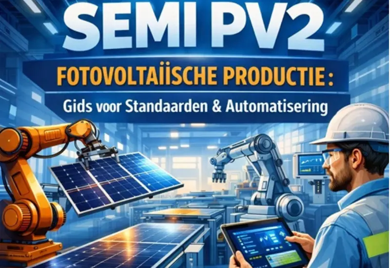
Inzicht in de SEMI PV2-standaard voor zonneproductie

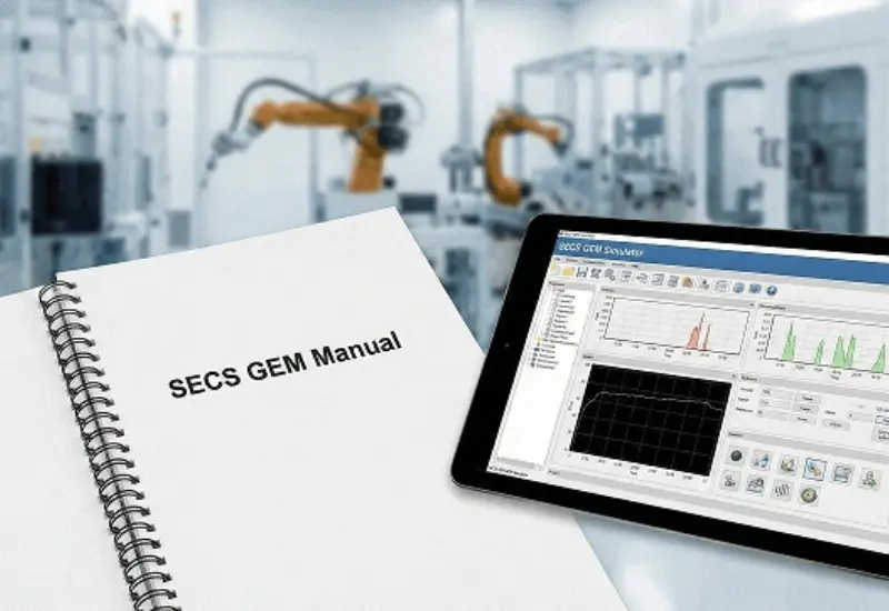
Het SEMI PV2-protocol, formeel bekend als de Specification for PV Equipment Communication Interfaces (PVECMS), definieert hoe apparatuur communiceert met fabrieksbeheersystemen. Het functioneert vergelijkbaar met SECS/GEM in de chipindustrie. Hoewel de halfgeleiderwortels duidelijk zijn, richt deze versie zich op de unieke hogesnelheidseisen van zonnecelproductie.

Standaardisatie voorkomt de “spaghetti-code”-valkuil. In plaats van maatwerkdrivers voor elk apparaat gebruiken engineers een plug-and-play-aanpak. Dit verkort de inbedrijfstelling van nieuwe productielijnen van maanden naar weken.

Kerncomponenten van PVECMS

Het PV2-framework focust op berichtstructuren: statusvariabelen, apparatuurconstanten en dataverzamelplannen. Bij fouten ontvangt het hostsysteem duidelijke, actiegerichte alarmen in plaats van vage codes.

Dataverzameling en traceerbaarheid

In een slimme fabriek heeft elke wafer een digitale tweeling. SEMI PV2 maakt gedetailleerde dataverzameling mogelijk in elke stap van doping en coating. Bij rendementsverlies kan de oorzaak worden herleid tot een specifieke thermische cyclus of depositiestap.

De rol van automatisering in fotovoltaïsche productie

Automatisering is de motor van de energietransitie. Handmatige omgang met fragiele siliciumwafers leidt tot breuk en variatie. Met automatisering bereiken bedrijven herhaalbaarheid die mensen niet kunnen evenaren.

Robots nemen het zware werk over: van het laden van kwartsboten in ovens tot eindtesten met elektroluminescentie. Dit verhoogt snelheid en veiligheid, vermindert fysieke belasting en beperkt menselijke contaminatie in de cleanroom.

Hogedoorvoer-handlingsystemen

Moderne zonnecellijnen verwerken soms meer dan 8.000 wafers per uur. Op deze snelheid kan zelfs een microseconde vertraging leiden tot een “wafer jam”. Door SEMI-gestuurde hogesnelheidsautomatisering worden zulke knelpunten voorkomen.

Visiesystemen en kwaliteitscontrole

AI speelt een sleutelrol bij inspectie. Geautomatiseerde vision-systemen detecteren microbarsten en pasta-defecten die het oog mist. Via PV2 wordt feedback direct teruggekoppeld voor onmiddellijke procesaanpassing.
Opmerking: Zelfs de beste robot faalt zonder interoperabiliteit—de geheime saus van hoge opbrengsten.

De slimme PV-fabriek bouwen

Een slimme fabriek is een levend systeem. Met PV-automatisering past zij zich aan haar omgeving aan—bijvoorbeeld door droogtijden te wijzigen bij veranderende luchtvochtigheid.

Dit vereist diepe integratie van SEMI-standaarden. Als machines dezelfde regels volgen, kan machine learning uitval voorspellen voordat die optreedt. De overgang van reactief naar voorspellend onderhoud is cruciaal voor winstgevendheid.

Industry 4.0 en de zonne-sector

De vierde industriële revolutie brengt gedecentraliseerde besluitvorming. Machines optimaliseren lokaal de flow, verlagen serverbelasting en verhogen robuustheid.

Is jouw fabriek slim of alleen snel? Een echte slimme fabriek gebruikt PV2-data voor simulaties—“what-if”-scenario’s testen procesparameters virtueel voordat materiaal wordt ingezet.

Voordelen van naleving van SEMI PV2-standaarden

Waarom certificeren? Voor markttoegang en betrouwbaarheid. Tier-1 afnemers vereisen vaak SEMI-conforme apparatuur—een vertrouwenslaag in een markt met dunne marges.

Lagere integratiekosten

Gestandaardiseerde interfaces verlagen integratiekosten. Minder tijd aan debugging, meer aan procesoptimalisatie—essentieel in een markt met voortdurende prijsdruk per watt.

Toekomstbestendige assets

De sector beweegt snel. SEMI PV2 is uitbreidbaar en laat nieuwe datatypen toe zonder complete herbouw van de software-architectuur.

Uitdagingen bij implementatie

De overgang naar volledige SEMI PV2-compliance kent obstakels. Oudere machines missen soms rekenkracht voor moderne stacks; “bridge”-apparaten vertalen legacy-signalen naar PV2-data.

Ook mensen zijn cruciaal. Engineers hebben nichekennis nodig op het snijvlak van software en industriële fysica—talent vinden blijft lastig.

Cybersecurity in de slimme fabriek

Meer connectiviteit betekent meer risico. SEMI-implementatie moet gepaard gaan met sterke netwerkbeveiliging om data te beschermen tegen spionage en aanvallen.

De toekomst van zonneproductiesystemen

We bewegen richting “lights-out” productie met minimale menselijke aanwezigheid. Toekomstige systemen gebruiken waarschijnlijk 5G voor ultralage latency.

Misschien voeden zonnepanelen straks de fabrieken die ze maken—een poëtische cirkel die absolute synchronisatie vereist. De drang naar efficiëntie stopt niet; standaarden wijzen de weg.

Conclusie

De energietransitie vraagt om schaalbare, hoogwaardige zonneproductie. Met SEMI PV2 ontstaat een fundament voor innovatie en betrouwbaarheid. Deze standaarden maken geavanceerde automatisering mogelijk en blijven cruciaal voor succes in slimme PV-fabrieken.

Contact Us Today

Krijg stapsgewijze hulp bij het implementeren van SEMI PV2-automatiseringsnormen


Enhancing Efficiency: Successful Deployment of Xpump on Edwards iGX100L

[vc_row][vc_column width=”1/2″][vc_column_text css=””]Product: Xpump by Einnosys
Company: A Leading Semiconductor Manufacturing Company in Singapore

Challenge:

The client, a prominent semiconductor manufacturing company in Singapore, was facing persistent challenges with their Edwards iGX100L dry pump system. The existing setup exhibited inefficiencies, including unoptimized performance, frequent maintenance needs, and unanticipated downtimes. These issues were negatively impacting the production process and adding significant costs. The company required a robust solution to enhance the dry pump’s reliability and performance, ensuring uninterrupted operations and achieving optimal throughput in their manufacturing lines.

Solution

Einnosys introduced its cutting-edge product, Xpump, as the solution to the client’s challenges. Xpump, known for its advanced features and seamless integration capabilities, was tailored to address the specific requirements of the Edwards iGX100L dry pump.[/vc_column_text][/vc_column][vc_column width=”1/2″][vc_single_image image=”35401″ img_size=”full” alignment=”center” css=””][/vc_column][/vc_row][vc_row][vc_column][vc_column_text css=””]Key Features Deployed

Real-Time Monitoring: Xpump’s advanced monitoring capabilities enabled real-time data tracking of pump performance, ensuring immediate detection of any anomalies.

Predictive Maintenance: The solution incorporated predictive maintenance features, reducing unplanned downtimes and extending the lifecycle of the Edwards iGX100L dry pump.

Energy Optimization: Xpump’s energy-efficient algorithms significantly reduced power consumption, aligning with the client’s sustainability goals.

User-Friendly Interface: A highly intuitive interface allowed operators to easily manage and control the dry pump system, minimizing training time and enhancing operational efficiency.

Seamless Integration: The product’s compatibility with the Edwards iGX100L ensured a smooth installation process with minimal disruption to the client’s manufacturing schedule.[/vc_column_text][vc_column_text css=””]Outcome

The implementation of Xpump delivered remarkable results for the client:

Enhanced Performance: The Edwards iGX100L dry pump exhibited significantly improved performance, operating at peak efficiency and meeting the rigorous demands of semiconductor manufacturing.

Reduced Downtime: The predictive maintenance features minimized unplanned breakdowns, ensuring uninterrupted operations and boosting overall productivity.

Cost Savings: The energy optimization capabilities of Xpump led to substantial reductions in power consumption, lowering operational costs.

Increased Reliability: The real-time monitoring and robust design of Xpump enhanced the reliability of the pump system, instilling confidence in the manufacturing process.

Improved Sustainability: By optimizing energy usage, the solution supported the client’s environmental initiatives and reduced their carbon footprint.[/vc_column_text][vc_column_text css=””]Feedback

The client expressed high levels of satisfaction with the Xpump implementation. Here’s what they had to say:

“Einnosys exceeded our expectations with Xpump’s AI/ML features, enhancing our Edwards iGX100L pump’s performance, efficiency, and reliability. Their professionalism from assessment to training was outstanding. We look forward to future collaborations.”[/vc_column_text][/vc_column][/vc_row]

AI in Semiconductor Equipment Automation: The Future of Fabs

Introduction

According to a report by McKinsey & Company (2022), artificial intelligence and machine learning could generate between $35 billion and $90 billion in annual value for the semiconductor industry. This massive financial potential stems from the way AI in semiconductor equipment automation addresses the extreme complexity of modern chipmaking. As transistors shrink to the size of a few atoms, the margin for error effectively vanishes, leaving human operators and static software unable to keep up.

The shift toward smart semiconductor manufacturing marks a departure from the “if-this-then-that” logic of the previous decade. Modern facilities produce terabytes of data every hour, yet much of that information previously sat idle in databases. Today, sophisticated algorithms digest these data streams to make split-second decisions that preserve wafer integrity and optimize throughput.

Equipment must now possess a level of “awareness” to handle the volatility of global supply chains and the precision required for sub-5nm nodes. By integrating AI-driven fab automation, manufacturers are discovering that they can push their hardware further than ever before. This evolution is less about replacing the equipment and more about giving the machinery a significantly better brain.

The Evolution of Autonomy in the Fab

Historically, semiconductor automation relied on rigid recipes. An engineer would program a tool to perform a specific action, and the tool would repeat that action until told otherwise. If a variable changed—such as a slight fluctuation in gas pressure or a rise in ambient temperature—the system often failed to adapt, resulting in scrapped wafers.

Breaking the Shackle of Static Recipes

The introduction of AI-driven fab automation changes this dynamic by allowing systems to learn from variance. Instead of following a hard-coded path, the equipment uses machine learning models to understand how different variables interact. If the software detects a slight drift in plasma density, it can automatically adjust the RF power in real-time to maintain the etch rate.

This level of flexibility is vital because modern chips are essentially 3D skyscrapers built on a microscopic scale. A single mistake on layer ten can ruin the entire structure by layer sixty. By moving toward smart semiconductor manufacturing, companies ensure that their tools are proactive rather than reactive.

Maximizing Uptime via Predictive Maintenance AI

Unscheduled downtime is the primary villain in any fab manager’s story. When a multi-million-dollar lithography tool goes offline unexpectedly, the cost can reach tens of thousands of dollars per hour. According to a study by Deloitte (2023), AI-based predictive maintenance can increase equipment uptime by up to 20% while reducing maintenance costs by 10%.

Listening to the Machines

Predictive maintenance AI works by analyzing vibration, thermal, and acoustic signatures from tool components. Every pump, motor, and robotic arm has a “healthy” frequency. When a bearing begins to fail, it emits a subtle change in vibration that a human would never notice.

The AI identifies these anomalies weeks before a catastrophic failure occurs. This allows the maintenance team to swap the part during a scheduled break. Have you ever wished your car could tell you exactly when the alternator was going to quit before you ended up stranded on the highway? In the semiconductor world, that wish is a functional reality.

Sensor Fusion and Data Correlation

The true power of predictive maintenance AI lies in sensor fusion. This involves correlating data from hundreds of different sensors to find hidden patterns. For example, a slight increase in power consumption combined with a minor decrease in cooling fluid flow might indicate a clogged filter. By identifying these correlations, equipment automation software prevents small issues from snowballing into factory-wide shutdowns.

AI-Driven Fab Automation and the War on Defects

Yield is the metric that keeps CEOs awake at night. In an industry where a 1% increase in yield can translate to millions in profit, the precision offered by AI in semiconductor equipment automation is indispensable. Automated Defect Classification (ADC) has undergone a radical transformation thanks to deep learning.

Beyond Human Sight

Traditional vision systems used simple pattern matching to find defects. However, as features become smaller, the “noise” in the images increases. AI-driven fab automation utilizes convolutional neural networks (CNNs) to distinguish between a harmless surface particle and a “killer defect” that will short-circuit the chip.

Ever see a grown engineer cry over a wafer scratch? It’s a sad sight, like a dropped ice cream cone, but worth fifty thousand dollars. AI reduces these tragedies by catching errors at the “point of inception,” stopping the production line before more wafers are tainted.

Real-Time Process Control (APC)

Advanced Process Control (APC) is the heart of smart semiconductor manufacturing. It uses AI to create a feedback loop between metrology tools and processing tools. If a measurement tool sees that a layer is slightly too thick, it immediately sends a command to the next tool in the sequence to adjust its timing. This “run-to-run” control ensures that the final product stays within the required specifications even if individual steps have slight variances.

The Core of Connectivity: Equipment Automation Software

No amount of artificial intelligence matters if it cannot talk to the hardware. This is where equipment automation software becomes the unsung hero of the fab. It acts as the translator between the high-level AI models and the low-level machine controllers.

Bridging the Protocol Gap

Most fabs run a mix of brand-new machinery and “vintage” tools that have been in service for decades. These older tools often speak older protocols like SECS/GEM. Modern equipment automation software provides a layer of connectivity that allows AI to extract data from these legacy systems.

Without this bridge, the fab would have “data islands” where information is trapped inside specific tools. By unifying the data stream, manufacturers can apply AI-driven fab automation across the entire production line, regardless of the age of the equipment.

Improving the User Interface

Automation software also simplifies the lives of engineers. Instead of staring at green-on-black terminal screens, they now interact with intuitive dashboards. These displays use AI to highlight the most critical information, ensuring that humans spend their time solving problems rather than hunting for data.

Smart Semiconductor Manufacturing as a Competitive Edge

The global semiconductor market is expected to reach $1 trillion by 2030, according to Statista (2024). In such a massive market, the winners will be those who can produce the highest volume with the lowest waste. Smart semiconductor manufacturing is no longer a luxury; it is a requirement for survival.

Companies that fail to adopt AI in semiconductor equipment automation will struggle with higher overhead and lower yields. The speed of innovation is simply too high for manual processes to remain viable. When your competitor is using AI to optimize their energy consumption and chemical usage, their cost per wafer will naturally be lower than yours.

Overcoming Implementation Hurdles

While the benefits are clear, moving to AI-driven fab automation is rarely a “plug-and-play” experience. It requires a fundamental shift in how data is managed. Many companies find that their data is messy, inconsistent, or stored in silos that the AI cannot access.

The first step is often a “data cleanup” phase. This involves standardizing how measurements are recorded and ensuring that every tool is properly calibrated. Once the foundation is solid, the equipment automation software can begin to feed the AI models the high-quality data they need to function.

Another challenge is the “black box” problem. Some engineers are hesitant to trust an algorithm if they cannot see how it reached a certain conclusion. To solve this, many developers are focusing on “Explainable AI” (XAI), which provides a rationale for the decisions the software makes. This helps build trust between the human operators and their digital partners.

Conclusion

The integration of AI in semiconductor equipment automation represents the most significant shift in chip manufacturing since the introduction of robotics. By embracing predictive maintenance AI and smart semiconductor manufacturing, fabs can achieve levels of efficiency and precision that were previously thought impossible. As the industry marches toward the trillion-dollar mark, the “brainpower” provided by equipment automation software and AI-driven fab automation will be the deciding factor in who leads the market.

Contact Us Today

Get Step-by-Step Guidance to Implement AI in Fab Automation


SECS GEM手册和模拟器

摘要 

  • 协议基础: SECS/GEM是连接半导体设备与工厂主机系统的标准语言,确保数据无缝交换。

  • 手册: 合适的手册将复杂的SEMI标准(E4、E5、E30)转化为可操作的规格,包括变量、报警和事件。

  • 模拟器: 使用模拟器对通信逻辑进行离线测试至关重要,可避免在价值数百万美元的实时工具上出现停机成本。

  • 集成步骤: 成功集成需要定义连接参数(IP/端口)、映射SVIDs/CEIDs,并进行严格的合规性测试。

  • 故障排除: 常见问题如T3超时通常由网络延迟或设备ID配置错误引起,模拟器可快速帮助识别。

引言 

半导体行业正经历复杂性和规模的巨大增长。根据SEMI(2024年),2023年全球半导体制造设备总销售额达到惊人的1063亿美元,推动力来自高性能计算和汽车芯片的需求。在现代千兆级晶圆厂中,依赖人工数据输入已不可行。机器必须与工厂主机顺畅通信,而这正是SECS/GEM手册和模拟器在工程师工具箱中最有价值的原因。

对于初学者来说,工厂自动化的“字母汤” SECS、GEM、HSMS、GEM300 可能令人不知所措。它听起来像只有穿着防尘服的人才能理解的秘密代码。然而,掌握SECS GEM通信不仅仅是记忆十六进制流,而是理解命令和控制的流程。无论您是试图让设备被晶圆厂接受的设备供应商,还是试图自动化老旧蚀刻机的工厂工程师,原理都是 样的。

本指南将去掉学术术语。我们将探索如何阅读规格说明、为什么没有强大的模拟器无法生存,以及如何像专家 样进行故障排除。

破解字母汤:什么是SECS/GEM?

在打开任何软件之前,我们必须先达成共识的语言。想象 个繁忙的餐厅厨房:厨师说法语,服务员说德语,经理说日语。结果必然是 片混乱。SECS/GEM就是半导体工厂车间的“英语”。

通信层级 

该协议实际上是由SEMI(国际半导体设备与材料协会)定义的 套标准堆栈。

  • SECS-I (SEMI E4): 传统方法,通过RS-232串行电缆通信,主要用于老旧设备。

  • HSMS (SEMI E37): 高速SECS消息服务,现代标准,通过以太网TCP/IP取代串行电缆,更快更可靠。

  • SECS-II (SEMI E5): 定义消息结构,例如“Stream 1, Function 1”表示“你在吗?”,“Stream 1, Function 2”表示“是,我在”。

  • GEM (SEMI E30): 通用制造设备通信与控制模型。SECS-II定义词汇,GEM定义语法与行为,规定机器如何启动、报告报警以及允许远程控制。

为什么晶圆厂要求它 

晶圆厂要求SECS GEM协议合规并非为了好玩,而是为了产量和效率。全自动300mm晶圆厂全天候运行。如果工艺工程师需要在50台设备上修改配方,他们不能手持U盘逐台操作,而是通过MES下达命令,由GEM接口完成其余操作。

导航SECS/GEM手册和模拟器 

购买软件许可证或设备集成套件时,通常会收到两样东西: 份厚重的PDF文档和 款软件。

手册:您的路线图 

“SECS/GEM手册”通常指工具接口的特定文档,通常称为EID(设备接口定义)。这是工具与主机之间的契约。

 份好的手册列出工具支持的每个“Stream”和“Function”,包括:

  • 状态变量 (SVIDs): 如腔室温度或压力等数据。

  • 设备常量 (ECIDs): 改变行为的设置,如超时。

  • 采集事件 (CEIDs): 告知主机发生某事件的触发器,例如“晶圆加工完成”。

手册不完善会导致集成变得困难,发送命令启动工艺时,机器可能因为缺少必要前置状态而无法响应。

模拟器:您的安全网 

绝不应在生产工具上直接测试代码,否则会收到愤怒的工厂经理电话。SECS/GEM手册和模拟器允许创建通信接口的“数字孪生”。

  • 如果你开发主机软件,模拟器就像设备端。

  • 如果你开发设备软件,模拟器就像工厂主机。
    它允许发送非法命令、触发虚假报警、虚拟断开电缆,从而观察软件如何恢复。

优秀模拟器的核心功能 

强大的日志记录与诊断 

当通信失败时,需要知道原因。优质模拟器提供详细事务日志,并将二进制SECS消息解析为可读文本(SML)。
提示: 选择能精确到毫秒的时间戳的模拟器,高速自动化中事件顺序非常重要。

脚本与自动化 

手动点击按钮发送消息适合第 天测试,但压力测试需要支持脚本的模拟器,例如:“每500毫秒发送 次‘状态请求’,持续24小时”,可发现手动测试无法发现的内存泄漏或时序问题。

GEM合规性验证 

工具是否真正遵循GEM标准?好的模拟器通常包含合规测试套件,检查通信是否正确建立、在线/本地与在线/远程切换是否正确,以及晶圆完成时事件报告是否发送。模拟器中失败成本为零,客户验收测试中失败可能损失数百万。

初学者流程:首次连接 

第1步:网络配置 

  • IP地址对齐

  • 设备(被动模式)监听特定端口(通常5000左右)

  • 主机(主动模式)发起连接

  • 设备ID: 标识工具的整数(0–32767),模拟器与工具ID不匹配将导致消息被忽略

  • T1, T2, T3定时器: 定义等待回复的时间,T3最关键(回复超时)

第2步:握手 (S1F13) 

  • 主机发送:S1F13(建立通信请求)

  • 设备回复:S1F14(确认通信)

  • 日志显示“CommAck = 0”表示连接成功

第3步:上线 

  • 工具通常初始为“离线”状态

  • 主机发送S1F17(请求上线),工具接受S1F18后即可控制设备

常见SECS/GEM问题排查 

T3超时 

  • 发送消息后设备未回复

  • 原因: 工具忙、网络延迟或软件崩溃

  • 解决: 检查网络ping,使用模拟器确认软件是否冻结

Function 0 (Abort Transaction)

  • 返回“SxF0”表示理解Stream但不支持Function

  • 原因: 请求未实现的功能

  • 解决: 查阅SECS/GEM手册

数据格式错误 

  • SECS对数据类型严格要求

  • 示例: 变量为2字节整数(I2),却发送4字节(I4)

  • 解决: 使用模拟器检查消息字节结构

超越基础:GEM300与未来 

掌握基础后进入GEM300世界,适用于300mm晶圆加工,包括复杂的自动物料搬运(AMHS)。模拟器对“载具管理”(FOUP装卸逻辑)测试至关重要。

根据麦肯锡(2023),全自动“无人工厂”的趋势加快,这意味着对可靠SECS/GEM通信的依赖只会增加。新协议如Interface A(EDA)用于高速数据采集,但SECS/GEM仍是指令和控制的核心。

结论 

进入半导体自动化世界学习曲线陡峭,但也是现代技术的核心。SECS/GEM手册和模拟器不仅是文档和软件,它们是机器与智能制造之间的桥梁。理解协议、利用强大模拟器测试并遵守标准,可确保价值数十亿美元的晶圆厂顺利运行。无论是调试T3超时,还是映射第 个采集事件,每 颗成功的芯片都始于 次成功的握手。

Contact Us Today

取得逐步指導,掌握 SECS/GEM 手冊與模擬器