Summary
- Modern semiconductor manufacturing demands extreme precision that manual processes fail to provide.
- Implementing semiconductor factory automation software can reduce operational costs by up to 20% while increasing throughput (McKinsey, 2023).
- Key technologies include SECS/GEM protocols, advanced MES integration, and AI-driven predictive maintenance.
- Automation minimizes human error in cleanroom environments, protecting delicate silicon wafers from contamination.
- The transition toward “Lights Out” manufacturing is a competitive necessity for 300mm fabs.
Introduction
According to McKinsey & Company (2023), AI and advanced analytics integrated into semiconductor factory automation software can reduce manufacturing costs by 15% to 20% for established fabs. This shift is essential as global demand for chips fluctuates, forcing facilities to find every possible margin for improvement. Efficiency is no longer a goal; it is a requirement for survival in a market where a single speck of dust or a millisecond of lag can ruin a million-dollar batch.
High-volume manufacturing requires a delicate balance of chemical precision, mechanical speed, and digital oversight. The introduction of robust fab automation solutions allows managers to oversee these complexities without constant manual intervention. By digitizing the workflow, companies ensure that every tool in the facility operates at its theoretical limit.
The current landscape of chip production is becoming more crowded and expensive. New facilities often cost upwards of $20 billion, making the software that runs them as valuable as the hardware itself. Adopting semiconductor factory automation software provides the backbone for these massive investments, ensuring that the return on investment remains high even as nodes shrink toward the sub-2nm frontier.
Why Software Defines the Modern Fab
Modern semiconductor manufacturing is less about the physical act of etching silicon and more about the data governing those etches. Human operators are remarkably talented, yet they are also walking biological contamination factories. A single skin cell can terminate a wafer’s journey. Automation software moves the human element away from the delicate front-end processes, placing them in control rooms where they can make strategic decisions rather than manual adjustments.
Eliminating the Human Variable
Does anyone actually miss the days of tracking wafer lots with physical clipboards and pens? Moving to a fully digital environment removes the risk of “fat-finger” errors where a technician might accidentally input the wrong recipe for a photolithography step. Software systems enforce strict compliance, ensuring that a tool will refuse to start unless the parameters match the pre-approved recipe perfectly.
Maximizing Equipment Effectiveness
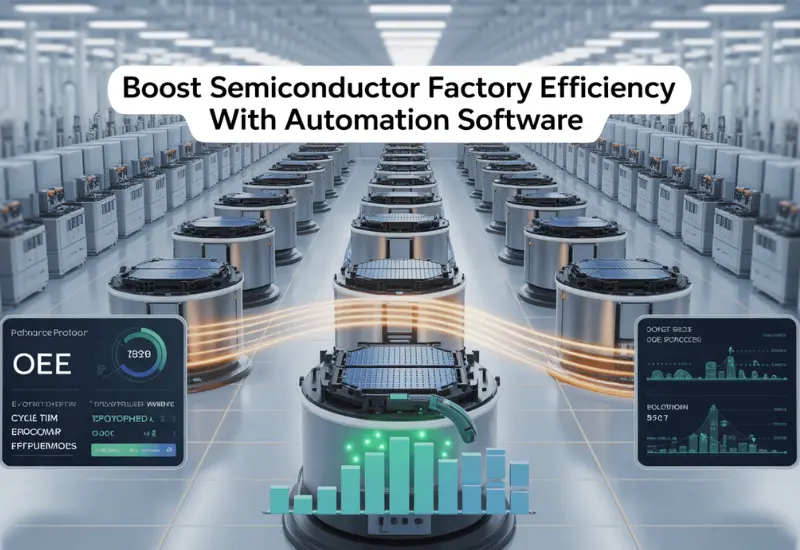
High-end tools like EUV lithography machines are too expensive to sit idle. Industrial automation software tracks Equipment Health Rating (EHR) and Overall Equipment Effectiveness (OEE) in real-time. If a tool begins to drift from its baseline, the software triggers an alert before the tool fails. This proactive approach changes maintenance from a reactive headache into a scheduled, predictable task.
Core Components of Semiconductor Factory Automation Software
A comprehensive software suite acts as the nervous system for a production facility. It connects the “brains” (the planning systems) to the “muscles” (the robotic arms and process tools). Without a unified layer of semiconductor factory automation software, a fab is simply a collection of expensive machines that speak different languages.
MES Software for Semiconductors
The Manufacturing Execution System (MES) serves as the central hub for all production activities. It tracks every wafer from the moment it enters the fab as a blank slate until it leaves as a finished die. MES software for semiconductors manages lot genealogy, ensuring that if a defect is found later, the team can trace it back to a specific tool or chemical batch.
Inventory and Material Handling
The movement of Front Opening Unified Pods (FOUPs) is a logistical puzzle. Automated Material Handling Systems (AMHS) rely on software to prioritize specific lots. If a high-priority customer order needs to jump the queue, the software reroutes the FOUPs across the ceiling-mounted tracks without causing a traffic jam in the cleanroom.
SECS/GEM and Connectivity
Communication protocols like SECS/GEM allow the software to talk to tools from different vendors. This standardization is what makes fab automation solutions viable. It creates a universal translator so that a South Korean etch tool and a Dutch lithography machine can both report their status to a centralized server in the United States.
Achieving Semiconductor Process Optimization
Efficiency is a game of inches or in this case, nanometers. Semiconductor process optimization involves analyzing thousands of data points per second to find bottlenecks. When software identifies that a specific chemical mechanical planarization (CMP) tool is taking 5% longer than its peers, engineers can intervene before that delay ripples through the entire line.
Real-Time Data Visualization
Data is useless if it stays buried in a database. Modern software provides dashboards that allow fab managers to see the status of the entire floor at a glance. Visualizing these workflows makes it obvious where wafers are stacking up. Often, a simple software tweak to the scheduling algorithm can clear a bottleneck that appeared to be a hardware limitation.
Digital Twins and Simulation
Some automation suites now offer “Digital Twin” capabilities. This allows engineers to test a new process recipe in a virtual environment before applying it to physical silicon. Testing in a sandbox environment prevents costly mistakes and speeds up the time-to-market for new chip designs.
The Role of AI in Industrial Automation Software
Artificial Intelligence is moving past the “hype” phase and into the practical phase. In the context of industrial automation software, AI acts as a 24/7 supervisor that never sleeps or needs a coffee break. It looks for patterns that are too subtle for a human eye to detect, such as a microscopic vibration in a robotic arm that precedes a total failure by three days.
Predictive vs. Preventive Maintenance
Preventive maintenance is like changing your car’s oil every 5,000 miles, regardless of how you drive. Predictive maintenance is like the car telling you exactly when the oil is dirty. By using semiconductor factory automation software with AI, fabs avoid replacing perfectly good parts, which saves money and reduces tool downtime.
Yield Enhancement via Machine Learning
Machine learning models analyze yield maps to find the “signature” of specific faults. If a cluster of dead chips appears on the edge of every wafer, the AI can correlate that pattern with a specific cooling vent in a furnace. This level of insight would take a human engineer weeks to find; the software does it in minutes.
Navigating the Challenges of Implementation
Switching to a new software architecture is a bit like performing heart surgery while the patient is running a marathon. Fabs cannot simply stop production for a month to install new code. The process must be incremental.
- Legacy Tool Support: Older tools might lack the sensors required for modern data collection.
- Data Silos: Different departments often use different software, making it hard to get a “single source of truth.”
- Cybersecurity: As fabs become more connected, they become bigger targets for industrial espionage.
- Skill Gaps: Automation requires a workforce that is as comfortable with Python as they are with physics.
Despite these hurdles, the cost of staying manual is far higher than the cost of upgrading. A fab that fails to automate will eventually find itself unable to compete with the yields and pricing of “Lights Out” facilities.
Future Trends in Semiconductor Automation
The industry is currently looking toward “Autonomous Labs” and edge computing. As we move closer to the physical limits of silicon, the software must become more autonomous. We are seeing a move toward decentralized control, where individual tools make localized decisions to optimize their own performance without waiting for a command from the central MES.
Visualizing a fab where the machines “negotiate” with each other for priority might sound like science fiction, but it is the logical conclusion of current trends. If an etch tool knows it has a filter change coming up, it can signal the lithography tool to slow down slightly to prevent a pile-up. This level of harmony is the ultimate goal of semiconductor factory automation software.
Conclusion
The complexity of modern chipmaking has surpassed the capacity of manual oversight. Facilities that embrace semiconductor factory automation software gain a massive advantage in yield, speed, and cost-efficiency. By integrating MES, AI, and standardized communication protocols, manufacturers can turn their facilities into highly tuned, data-driven engines of production. If you want to keep your fab competitive in an era of shrinking nodes and rising costs, the software is your most important tool.
Get Professional Support to Optimize Production and Reduce Downtime