FAB自动化制造自动化

摘要

  • SECS/GEM 是半導體設備與主機系統通訊的核心標準,確保資料一致性與可追溯性。

  • GEM 消除客製化整合問題,讓設備能以統一方式上報事件、警報、資料與配方。

  • 透過標準化的設備狀態模型、事件與資料收集機制,大幅縮短設備導入時間。

  • GEM 的功能涵蓋遠端控制、警報管理、配方下載/上傳、資料收集與設備監控。

  • SECS/GEM 是實現工廠自動化、提升良率、加速量產與支援 MES/APS/調度系統的基礎。

簡介

根據麥肯錫 2023 年報告,全球半導體市場預計在 2030 年成為兆美元產業。
但隨著製程節點縮小、晶圓成本飆升,容錯空間幾乎消失,人力已無法支撐高度精密的需求。
這正是 FAB 自動化的價值所在。
現代晶圓廠需要協調數千個製程步驟、處理 TB 級資料,並讓價值數十億美元的工廠穩定運作。

硬體主軸:無人搬運晶圓

最明顯的自動化系統是 AMHS。走進 300mm 晶圓廠,你會看到天花板上的高速軌道,而不是人類搬運 FOUP。

OHT 天車運輸系統

OHT 就像晶圓的電動計程車,在天花板軌道上移動,精準將晶圓批次送達指定工具。
它必須高速、精準並維持超低震動,才能保護價值數萬美元的晶圓。

EFEM 與 Load Port

OHT 將 FOUP 送到機台後,由 EFEM 接手。
EFEM 提供比無塵室更潔淨的局部環境,並透過機械手臂將晶圓送入製程腔體。
這徹底排除人為污染風險,使晶圓全程保持在最佳環境。

 軟體大腦:連接整個製程

晶圓廠硬體需要軟體指揮。這套軟體架構就像軍事指揮鏈,一層接一層。

MES 製造執行系統

MES 是工廠的「指揮官」。
它負責:
• 工單管理
• 庫存追蹤
• 排程與派工
• 決定哪一批晶圓要進入哪一台工具

EAP 設備自動化控制

EAP 是 MES 的「翻譯官」。
它將 MES 指令轉為機台能理解的語言,並處理:
• 配方驗證
• 執行中資料收集
• 警報處理
沒有 EAP,機台變成「笨機器」,需要操作員手動輸入配方,非常容易造成報廢。

How Fab Automation Transforms Production

SECS/GEM 設備通訊標準

SECS/GEM 是晶圓廠通訊的「USB 標準」。
它讓不同廠牌機台以相同方式通訊,是當今最普及的控制標準。
雖然 EDA(Interface A)已用於高速資料收集,但 SECS/GEM 仍是主要控制協定。

工業 4.0:當資料變成行動

現代 FAB 自動化已不只是控制,而是預測並優化。

預測性維護 (PdM)
AI 可分析震動、聲音與溫度等感測資料,提前預測設備故障。
不再依照固定時程更換零件,而是根據實際狀況維修,避免突發停機與報廢。

數位孿生

工程師可建立晶圓廠的虛擬複製體,模擬物料流動、工具交互與 OHT 交通。
例如:新增機台是否會造成 OHT 壅塞?
只需在數位孿生中模擬即可得知。

自動化晶圓廠的挑戰

老舊設備整合問題

晶圓廠設備價格昂貴,許多工具使用 10–20 年以上。
這些老機台缺乏感測器與運算能力,需藉助 IoT Gateway 或改裝控制器來與系統整合。

整合成本

全面自動化需要高額初期投資,但帶來更高良率、低人力成本與更穩定的產能。

人類角色轉變

自動化不是取代人類,而是讓人類從「操作者」轉為:
• 維護專家
• 數據分析師
• 製程優化工程師

結論

FAB 自動化是推動半導體邁向兆美元產業的核心力量。
整合 OHT、EFEM 等硬體與 MES/EAP 等軟體,能讓工廠達到未來製程所需的精密度。
無論是改造舊機台或規劃新

Contact Us Today

取得逐步協助,實現您的晶圓廠製造自動化

How to Market & Sell Semiconductor Equipment Performance Software

Summary

  • Lead with data-backed ROI by highlighting specific gains in yield, throughput, and uptime rather than using vague efficiency claims.
  • Prioritize SECS/GEM connectivity to ensure your software integrates seamlessly with existing factory automation protocols.
  • Navigate long sales cycles of 6 to 18 months by building trust through multi-layered stakeholder engagement and technical proofs of concept.
  • Address risk aversion directly by demonstrating cybersecurity compliance and the ability to work with both legacy and modern equipment.
  • Use technical marketing assets like white papers and API guides to build authority with the engineering teams who influence buying decisions.

Introduction

According to a 2024 report by SEMI, global semiconductor equipment sales are projected to reach a record $124 billion by 2025 (SEMI — 2024). This massive capital expenditure highlights a critical need for performance improvement software for semiconductor equipment as manufacturers strive to maximize the output of their multi-million dollar assets. Selling into this space requires a blend of deep technical fluency and an understanding of the immense pressure found on the cleanroom floor.The right software directly improves yield and throughput, turning operational data into measurable production gains.

Success in this niche requires more than a standard pitch deck; it demands a proof-of-value that resonates with both the C-suite and the floor engineers. In an environment where a single hour of downtime costs a leading fab upwards of $30,000, software is no longer a peripheral concern (McKinsey — 2023). It is the primary driver of competitive advantage.

Building a robust pipeline for semiconductor software sales means speaking the language of throughput, uptime, and yield. Whether you are marketing to Original Equipment Manufacturers (OEMs) or directly to the fabs, your strategy must reflect the precision of the hardware your software controls.

Understanding the Unique Sales Cycle of Fab Equipment

Marketing to the semiconductor industry is a marathon, a sprint, and an obstacle course combined. The buying process often involves multiple layers of stakeholders, from procurement officers to automation specialists who treat their equipment like a prized collection of high-tech sports cars.

Selling to OEMs vs. Fabs

OEMs look for OEM software solutions that make their machines more attractive to end-users. They want reliability and ease of integration. If your software makes their hardware look better, you have a deal. Conversely, fabs focus on fab equipment optimization tools that can be retrofitted or integrated into existing workflows to squeeze out an extra 1% of efficiency.

The Role of Long-Term Proof of Concept (PoC)

Technical teams rarely take a salesperson’s word for it. A PoC is the standard “prove it” phase. During this time, the software must demonstrate its ability to handle high-volume data without crashing the host system. Highlighting how your manufacturing efficiency software handles real-world variability is essential for moving past the trial phase.

Positioning Performance Improvement Software for Semiconductor Equipment

To market your product effectively, you must define what “performance” actually means for a fab. Is it faster wafer handling? More precise chemical delivery? Or perhaps it is the reduction of “ghost” alarms that stop production for no reason.

Marketing SECS/GEM Software Connectivity

Modern fabs run on data, and that data flows through SECS/GEM protocols. When engaging in SECS/GEM software marketing, focus on the seamless nature of your integration. If an engineer thinks they have to spend six months coding a bridge to your software, they will walk away. Emphasize “plug-and-play” capabilities, even if the reality involves a bit more configuration.

Solving the Data Silo Problem

Many fabs suffer from “islands of automation” where machines do not talk to each other. Your marketing should highlight how your performance improvement software for semiconductor equipment breaks down these barriers. Connectivity is the foundation of any optimization effort.

Data-Driven Strategies for Manufacturing Efficiency Software

Gartner (2023) reports that 60% of manufacturing organizations will utilize digital twins or advanced simulation to optimize production by 2026. This trend provides a perfect opening for software vendors.

Quantifying the ROI of Optimization

Numbers talk louder than adjectives in this industry. Instead of saying your software is “fast,” state that it reduces wafer cycle time by 4.2 seconds. This level of specificity builds immediate credibility. Use case studies to show how fab equipment optimization tools directly impact the bottom line.

Addressing Technical Debt and Legacy Systems

Many fabs still run on hardware that belongs in a museum, yet it produces millions of dollars in chips. Selling performance software often involves convincing a manager that your modern code can coexist with a 20-year-old PLC. Marketing materials should address compatibility directly to alleviate the fear of broken workflows.

Overcoming Resistance in Semiconductor Software Sales

The semiconductor world is notoriously risk-averse. If a machine is working, no one wants to touch it. This “if it ain’t broke, don’t fix it” mentality is the biggest hurdle for semiconductor software sales.

The Security Objection

With intellectual property worth billions, fabs are paranoid about cybersecurity. Ensure your sales team can discuss “air-gapped” environments and data encryption with ease. If your software requires a constant cloud connection, be prepared for a very short meeting.

The Ease of Use Factor

Engineers are busy. If your software requires a 200-page manual to operate, it will become shelfware. Marketing should highlight intuitive dashboards and automated reporting features. Think of it like a “check engine” light, but for a $50 million lithography machine—simple, clear, and actionable.

Advanced Marketing Channels for OEM Software Solutions

Traditional ads rarely work in the semiconductor space. You are not selling soap; you are selling a complex logic system.

  • White Papers: Deep dives into specific technical challenges (e.g., thermal management or vacuum stability).
  • Webinars with Industry Experts: Partnering with a known consultant can lend your brand instant authority.
  • Trade Shows: Events like SEMICON are where the real networking happens.

Content Strategy for Automation Specialists

Automation specialists value technical documentation over flashy brochures. Provide them with API references, integration guides, and performance benchmarks early in the sales process. This transparency fosters trust and shortens the evaluation period.

Crafting the Final Pitch

When the time comes to close the deal, the focus should return to the human element. The fab manager is not buying code; they are buying a better night’s sleep. They want to know that when they go home, the machines will keep humming along.

A successful pitch for performance improvement software for semiconductor equipment connects the technical specs to the emotional relief of a stable production line. Use testimonials from other engineers to provide social proof. In a small industry like this, reputation is everything. One successful installation at a major fab can lead to a dozen more through word-of-mouth.

Conclusion

Marketing and selling performance improvement software for semiconductor equipment requires a deep respect for the complexity of the manufacturing environment. By focusing on data-driven ROI, seamless connectivity, and robust security, your sales team can overcome the industry’s natural resistance to change. As the demand for smaller, faster chips grows, the software that optimizes their production will become the most valuable tool in the cleanroom.

Contact Us Today

Get Expert Guidance to Sell Performance Software to Semiconductor Fabs

Taking the next leap forward in semiconductor yield improvement

Summary

Economic Context: With semiconductor revenue projected to hit $629.8 billion (Gartner, 2024), yield optimization remains the most significant driver of fab profitability.

Strategic Shift: Modern facilities are moving from reactive firefighting to proactive, data-driven yield improvement via real-time analytics.

Key Pillars: Successful yield enhancement relies on advanced metrology, machine learning for wafer map analysis, and rigorous process optimization in semiconductor manufacturing.

Future Readiness: Integrating AI and automated fab yield analytics allows engineers to identify root causes of defects before they compromise entire production lots.

Introduction

According to Gartner (2024), worldwide semiconductor revenue is projected to grow 18.8% to reach $629.8 billion. This massive expansion puts immense pressure on production facilities to minimize waste while accelerating output. Effective semiconductor yield improvement serves as the primary lever for maintaining profitability while meeting this skyrocketing demand.

As chips become more complex, the margin for error shrinks. A single airborne particle or a microscopic misalignment during lithography results in millions of dollars in lost revenue. Consequently, the industry is seeing a shift toward more sophisticated, automated solutions to manage these complexities.

Facilities that fail to adapt their yield management protocols face mounting losses. High-volume manufacturing requires a delicate balance of speed and precision that manual oversight can no longer provide. By embracing modern yield improvement strategies, fabs can secure their position in an increasingly competitive global market.

The Financial Reality of the Modern Fab

In the world of microchip fabrication, yield is the ultimate metric of health. It represents the percentage of functional devices produced compared to the maximum possible number on a wafer. When manufacturing costs for a single 300mm wafer can reach several thousand dollars, every percentage point of yield translates directly to the bottom line. According to SEMI (2024), global 300mm fab equipment spending is expected to reach $137 billion by 2027, highlighting the massive capital at stake.

Why 99% is the New Failure

In legacy nodes, a 90% yield might have been acceptable. However, for leading-edge nodes (5nm and below), the complexity of multi-patterning and 3D structures like Gate-All-Around (GAA) transistors makes achieving high yield significantly harder. A yield rate that lingers below targets for too long can bankrupt a product line before it even reaches the consumer market.

The Cost of Yield Excursions

A yield excursion, a sudden, unexpected drop in productivity, is the nightmare of every fab manager. These events often stem from equipment drift, contaminated chemicals, or software glitches in the automation layer. Rapid identification through fab yield analytics is essential to prevent these excursions from turning into month-long shutdowns.

Strategic Pillars for Semiconductor Yield Improvement

Improving output requires a multi-layered approach that addresses both the physical environment and the digital data stream. Engineers must look beyond the immediate defect and analyze the systemic issues within the production line.

Data-Driven Yield Improvement

Modern fabs are essentially giant data factories. Every tool on the floor generates a constant stream of telemetry. Data-driven yield improvement involves aggregating this information into a centralized “single source of truth.” By correlating sensor data with electrical test results, engineers find hidden patterns that human observation would miss.

Machine Learning and Wafer Map Analysis

Machine learning algorithms excel at recognizing defect patterns. If a specific cluster of “killer defects” appears in the same spot on every fifth wafer, the AI can trace this back to a specific robot arm or a cooling vent. This level of semiconductor manufacturing yield analysis moves the needle from “what happened” to “why did it happen.”

Yield Optimization in Fabs Through Metrology

Metrology, the science of measurement, is the backbone of quality control. Advanced optical and electron-beam inspection tools allow for real-time monitoring of wafer health. Implementing high-speed inspection at critical steps ensures that a flawed wafer is pulled from the line early, saving the costs of subsequent processing steps.

Process Optimization in Semiconductor Manufacturing

Refining the actual chemical and physical steps of production is where the hardest work occurs. This involves a constant feedback loop between the R&D team and the floor engineers.

Reducing Defect Density

Defect density is the number of defects per unit area. As die sizes grow for high-performance computing (HPC) chips, the probability of a defect landing on a functional area increases. Process optimization in semiconductor manufacturing focuses on “cleaning up” the process by stabilizing plasma etching, refining chemical mechanical polishing (CMP), and ensuring ultra-pure water systems remain pristine.

Advanced Process Control (APC)

APC systems automatically adjust tool parameters in real-time. If a sensor detects a slight rise in temperature during a deposition step, the APC system compensates by adjusting the gas flow or pressure. This prevents the process from drifting outside of the specified tolerances, maintaining a steady semiconductor manufacturing yield.

Overcoming Human and Environmental Factors

Engineers in bunny suits often resemble confused astronauts, yet their focus on particulates is deadly serious. Human error remains a significant contributor to yield loss, whether through improper tool handling or simple data entry mistakes.

The Role of Fab Automation

Automation reduces the number of human-wafer interactions. Automated Material Handling Systems (AMHS) transport wafers in sealed FOUPs (Front Opening Unified Pods), drastically lowering the risk of contamination. When the human element is minimized, the consistency of the process increases. Is it possible to reach “lights-out” manufacturing? While a fully autonomous fab is still a future goal, the industry is closer than ever.

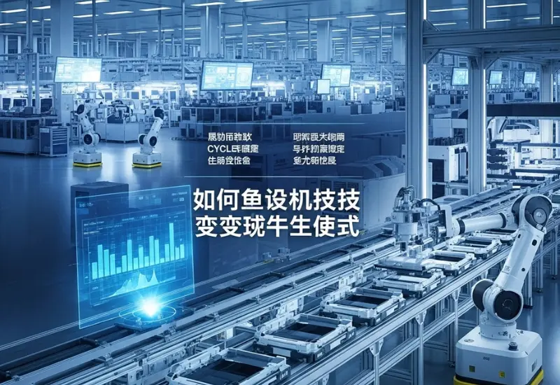
Implementing Advanced Fab Yield Analytics

To take the next leap, fabs must transition from descriptive analytics (what happened) to prescriptive analytics (what should we do). This requires a robust software infrastructure capable of handling massive datasets without latency.

Identifying Spatial Signatures

Often, yield loss is not random. It follows a spatial signature like a ring around the edge of the wafer or a streak across the middle. Fab yield analytics tools can automatically classify these signatures. For instance, a “donut” pattern might indicate an issue with the gas distribution plate in a CVD (Chemical Vapor Deposition) chamber.

Shortening the Learning Cycle

The time it takes to find a problem, fix it, and verify the fix is known as the learning cycle. In a traditional setup, this might take weeks. With integrated yield improvement strategies, this cycle is compressed into days or even hours. This speed is vital when ramping up a new process node.

The Future of Yield Management

The next decade will see even tighter integration between design and manufacturing. Feedback loops will extend back to the chip designers, who will receive real-time data on which structures are failing most frequently. This “closed-loop” system will make semiconductor yield improvement a collaborative effort across the entire supply chain.

According to a McKinsey (2022) report, the semiconductor industry is on track to become a trillion-dollar industry by 2030. Reaching that milestone requires a relentless focus on efficiency. Facilities that prioritize data-driven yield improvement will be the ones that capture the lion’s share of that growth.

Do we really expect machines to manage themselves? In many ways, they already do. The shift toward “smart” factories means that the role of the yield engineer is changing from a data gatherer to a high-level strategist who oversees complex AI ecosystems.

Conclusion

Mastering semiconductor yield improvement is a journey of constant refinement rather than a final destination. By integrating advanced fab yield analytics and rigorous process optimization in semiconductor manufacturing, facilities can navigate the complexities of modern chip production. The combination of human expertise and machine intelligence ensures that every wafer produces the maximum number of functional dies, securing both profitability and technological progress.

Contact Us Today

Get Step-by-Step Help to Improve Semiconductor Yield


Pengenalan SECS GEM

SECS (Piawai Komunikasi Peralatan SEMI) / GEM (Model Peralatan Generik) adalah protokol antara muka komunikasi untuk komunikasi antara peralatan semikonduktor dan host fab. Fab host adalah aplikasi perisian yang mengawal dan memantau pemprosesan peralatan menggunakan protokol SECS / GEM. Peralatan yang mematuhi SECS / GEM dapat berkomunikasi dengan host fab menggunakan TCP / IP (menggunakan standard SEMI E37 dan E37.1 – HSMS) atau RS-232 (menggunakan SEMI standard E4 – SECS-I). Antara muka standard SECS / GEM digunakan untuk memulakan serta menghentikan pemprosesan peralatan, mengumpulkan data pengukuran, memilih resipi untuk produk dan mengubah pemboleh ubah. Dengan SECS / GEM, semua ini dapat dilakukan dengan cara standard. Protokol SECS / GEM telah diseragamkan oleh SEMI persatuan bukan untung (Peralatan dan Bahan Semikonduktor Antarabangsa). Lihat www.SEMI.org untuk mengetahui lebih lanjut mengenai standard SEMI dan protokol SECS / GEM.

Dengan kata mudah, standard SECS / GEM mentakrifkan mesej, mesin keadaan dan senario untuk membolehkan aplikasi host kilang mengawal serta memantau peralatan pembuatan. Piawaian GEM secara rasmi ditetapkan sebagai standard SEMI E30, tetapi sering disebut sebagai standard GEM atau SECS / GEM. GEM bermanfaat untuk kedua-dua pengeluar peranti dan pembekal peralatan kerana ia menentukan sekumpulan kelakuan peralatan dan keupayaan komunikasi yang sama untuk menyediakan fungsi serta fleksibiliti untuk menyokong pembuatan. Oleh kerana standard GEM hanya mempunyai beberapa ciri khusus semikonduktor, ia telah diadopsi oleh industri pembuatan lain juga, seperti PV.

Antara keupayaan yang ditawarkan oleh standard SECS / GEM adalah –

Untuk hos fab memulakan dan menghentikan pemprosesan

Agar tuan rumah fab memilih, memuat turun, dan memuat naik resipi dari / ke peralatan

Untuk tuan rumah fab untuk meminta peralatan untuk nilai dari pelbagai parameter proses dan konfigurasi peralatan

Untuk host fab untuk menetapkan nilai parameter konfigurasi peralatan

Untuk peralatan menghantar penggera ke host fab

Untuk tuan rumah fab untuk menentukan laporan pelbagai pemboleh ubah dan mengaitkannya dengan peristiwa seperti permulaan banyak atau wafer selesai

Oleh kerana SECS / GEM adalah protokol komunikasi, ia adalah platform dan teknologi serta bahasa pengaturcaraan tidak bergantung. Bahagian host sambungan dijalankan pada sistem komputer yang disediakan oleh kilang, dan bahagian peralatan sambungan dijalankan pada komputer pengawal yang disediakan oleh pengeluar peralatan. Ini memberikan kedua-dua fungsi dan kebolehpercayaan pengeluar peralatan, fleksibiliti dan kebebasan platform. Keduanya, fab dan OEM dapat mengembangkan aplikasi perisian mereka tanpa perlu bimbang tentang keserasian komunikasi, asalkan kedua-duanya mematuhi standard SECS / GEM.

eInnoSys menawarkan penyelesaian perisian SECS / GEM untuk pengeluar peralatan (OEM) dan juga kilang (FAB atau ATM). Dengan mengintegrasikan perisian plug-n-play EIGEMEquipment eInnoSys dengan perisian alat kawalan peralatan, OEM dapat mengurangkan kos dan masa yang diperlukan untuk menjadikan peralatan mereka mampu SECS / GEM. Begitu juga, EIGEMHost adalah perisian SECS / GEM untuk FAB dan ATM (Pemasangan dan Ujian Pembuatan) untuk berkomunikasi dengan pelbagai peralatan di kilang. EIGEMSim adalah perisian simulator untuk ujian SECS / GEM. Ini adalah perisian yang boleh dikonfigurasi sebagai host atau peralatan untuk menguji komunikasi SECS / GEM yang lain.

SECS menerangkan komunikasi antara komputer hos dan peralatan menggunakan satu sambungan. Dalam konsep asal dan bahkan hari ini dalam senario yang paling biasa, peralatan menyediakan antara muka SECS tunggal untuk penggunaan eksklusif oleh satu hos. Jenis mesej yang ditentukan oleh SECS sebahagiannya tidak simetri – beberapa jenis mesej didefinisikan hanya untuk penggunaan host, yang lain hanya ditentukan untuk peralatan, tetapi juga banyak dari mereka didefinisikan untuk penggunaan yang sama di kedua-dua belah pihak.

Namun, terdapat peruntukan dalam standard SECS untuk berkongsi sambungan dengan menentukan nilai pengenalan peranti dalam setiap mesej. Amalan perkongsian sambungan tidak digalakkan untuk penggunaan baru. Adalah menjadi kebiasaan bahawa sambungan dijaga untuk jangka masa yang panjang dan hanya terganggu jika peralatan atau hos dihidupkan semula. Sambungan SECS ringan dan tidak menggunakan lebar jalur rangkaian yang banyak. Adalah mungkin untuk menjalankan beberapa sambungan SECS pada komputer desktop biasa.

半導體設備通信標準

當我們談論SEMI,SECS和GEM時。首先讓我們了解這些縮寫是什麼。

SECS指半導體設備通信標準,GEM指製造設備通信和控制的通用設備模型,SEMI代表半導體設備材料倡議。

半導體設備材料倡議(SEMI)開發了一套稱為SECS / GEM的標準。這些標準用於定義自動化設備和主機之間的一組通信協議。

SEMI標准在1970年代某個地方出現。引入這種標準背後的想法是支持小型但蓬勃發展的半導體行業。 SEMI帶來了各種半導體設備和Fab主機之間的通信協議標準。這就消除了對特定於設備或Fab主機的通信規範的需求。這樣,這些標準類似於如何為網絡通信定義TCP / IP協議或為串行通信定義RS232。

早期,沒有標準的過程可以處理半導體設備和Fab主機之間的通信。這曾經導致半導體行業的高成本和低性能。因此,這就需要採用標準流程來解決這種情況。那就是SECS / GEM的SEMI標準誕生的地方。

SECS / GEM標準必須同時在主機和設備上實施。設備在其分配的計算機上運行軟件,該軟件實現並符合各種SEMI標準,例如E30,E4,E5和E30。同樣,工廠運行需要實施必要軟件以實現完全相同的SEMI標準的主機軟件,以便它可以與設備以相同的“語言”進行通信。

更多細節